SRAM-based 4-bit MAC
A 6T bitcell, a 16×4 SRAM, and a 4-bit MAC in Cadence GPDK 18 nm at 0.8 V. Seventeen cycles from START to DONE.
0.39 µm² cell · 0.69 ns SRAM · 2.5 ns MAC. Part 1 is extracted; Parts 2 and 3 are schematic-level.
The unit computes \(\mathrm{ACC}=\sum_{i=0}^{15} W_i X_i\) from two copies of the Part 2 macro, a 4×4 array multiplier, a 12-bit ripple accumulator, and a 4-bit counter plus FSM. Every register is a transmission-gate master-slave flip-flop. ESE 5700 Project 1, University of Pennsylvania.
Start with the specification, then the bitcell, the SRAM macro, and the MAC. Estimates are labeled. Full write-ups:
1. Specification
The unit computes a 16-element dot product of 4-bit unsigned weights \(W\) and activations \(X\):
The maximum unsigned sum is \(16\times15\times15=3600\), which fits in 12 bits. Two copies of the Part 2 16×4 macro hold W and X. A static-CMOS 4×4 array multiplier, a 12-bit ripple-carry accumulator, a 4-bit address counter and a two-bit controller sequence the 16 products. Every register is a transmission-gate master-slave flip-flop. The read is pipelined against the multiply-accumulate (address and read in cycle n, accumulate in n+1), so a dot product takes 17 cycles from START to DONE (handout limit: 20).
| Part | Deliverable | Due | In repo |
|---|---|---|---|
1 |
6T bitcell: schematic, custom layout, post-layout stability |
10/13/2026 |
Cell 0.39 µm², DRC 0, LVS clean; extracted read SNM 140 mV at 0.8 V |
2 |
Cell tiled into a 16 × 4 synchronous SRAM macro |
10/20/2026 |
\(T_{CLK}=0.69\) ns, \(t_{\mathrm{access}}=488\) ps, area 54.6 µm² (est.), FOM \(\approx 4.7\times10^{3}\) |
3 |
Two macros + datapath + sequencer → MAC |
10/27/2026 |
\(T_{CLK}=2.5\) ns, \(t_{dot}=42.5\) ns, Test A 8.870 pJ, FOMMAC \(=1.1\times10^{5}\) |
1.1. Technology and flow
-
Cadence GPDK 18 nm, Virtuoso schematic and (Part 1) custom layout.
-
Spectre / ADE / ViVA. Part 1 characterization is extracted. Parts 2 and 3 in this report are schematic-level (no extracted parasitics on the MAC).
-
Nominal \(V_{DD}=0.8\,\mathrm{V}\), 27 °C. Part 1 also reports 0.7 V and 0.5 V.
-
Density factor \(D=28\) from the laid-out cell: one fin = 0.048 µm × 18 nm = 0.0242 µm².
Full handout: course project handout.
1.2. Repository map
| Path | Owns |
|---|---|
|
Part 1 Gradescope report |
|
Part 2 report, cropped figures |
|
Part 3 report and |
|
This site |
|
Official handout |
|
Bitcell schematic, layout, butterflies |
|
Raw SNM CSVs |
|
Part 2 unit-test notes (write driver, decoder, macro) |
1.3. Flow checkout (sample inverter)
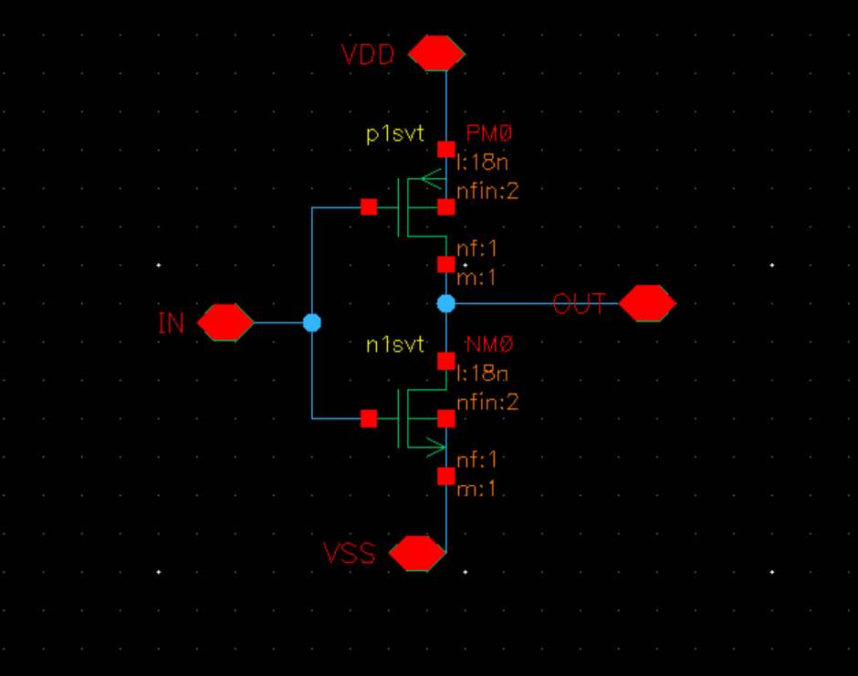
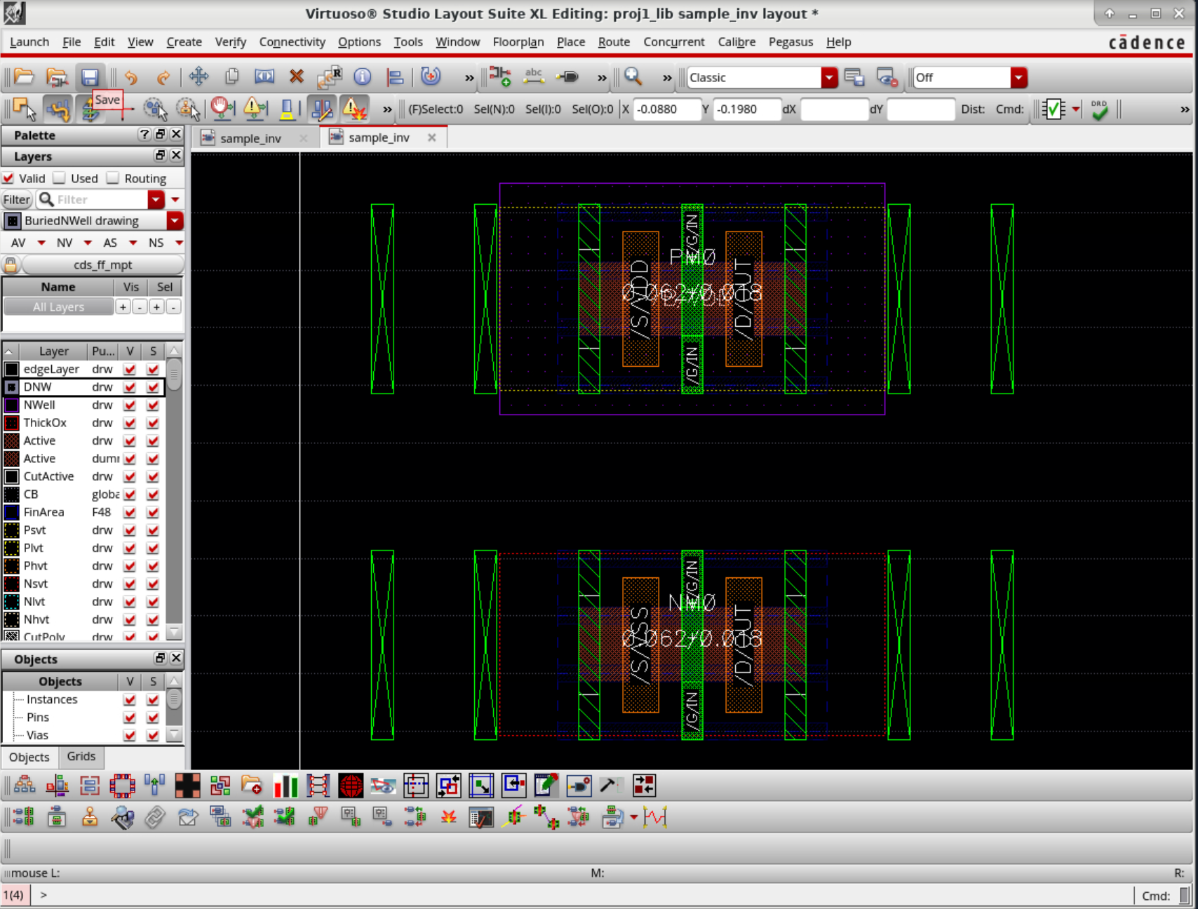
Before the bitcell, the Cadence environment is checked out with a sample inverter (proj1_lib sample_inv).
2. Assignment and evidence
The current handout sets the project in GPDK 18 nm at nominal 0.8 V and requires one team PDF per part. Part 1 asks for a symmetric cell, hand sizing, a three-value schematic β sweep, a DRC/LVS-clean tileable layout, parasitic extraction, post-layout stability, supply dependence and a functional write/read. Parts 2 and 3 add the 16×4 macro and the MAC. Each report names both members and their contributions.
2.1. What is recorded
-
Virtuoso 6T schematic with PD/PG/PU fin counts; handwritten read/write analysis; β=1 / 1.5 / 2 SNM CSVs and original ViVA butterflies.
-
Layout area, DRC 0, LVS match, extracted \(C_{BL}=180\) aF / \(C_{WL}=90\) aF, post-layout SNM and write margin (Layout, extraction and post-layout results).
-
Part 2 macro benches: write driver nfin=8, decoder,
tb_sram_macroaccess and power (SRAM macro (Part 2)). -
Part 3
tb_topTests A/B/C, DFF characterization, multiplier 256/256, controller 60/60, energy and FOM (MAC unit (Part 3)).
2.2. Evidence level
Part 1 numbers on this site that come from Quantus are extracted. Part 2 and Part 3 timing, energy and area (except the tiled cell) are schematic-level or \(D\sum W_i L_i\) estimates and are labeled as such. A hand estimate never stands in for a measured Spectre integral.
3. Cell schematic and dimensions
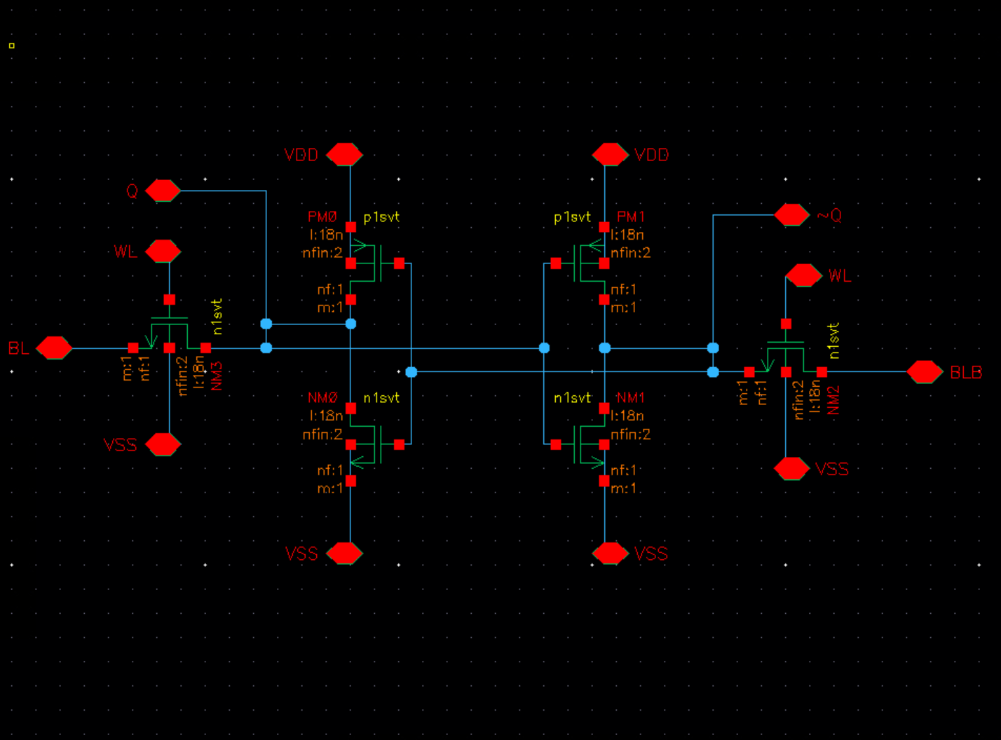
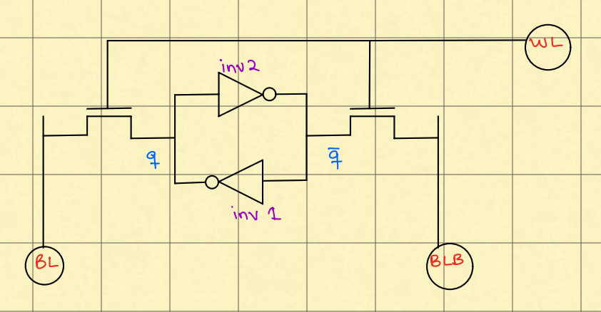
The 6T cell consists of two cross-coupled inverters and two pass-gates. During a read, asserted WL connects both storage nodes to precharged BL/BLB. During a write, the bitline drivers force complementary values through the pass-gates. The schematic keeps both halves symmetric.
| Device | Each side | Role |
|---|---|---|
Pull-down NMOS (PD) |
4 fins, L=18 nm |
Holds a stored zero against read disturb |
Pull-up PMOS (PU) |
2 fins, L=18 nm |
Holds a stored one; opposes a write-zero |
Pass-gate NMOS (PG) |
2 fins, L=18 nm |
Connects the storage node to its bitline |
With equal nominal channel lengths, the intended ratios are \(\beta=(W/L)_{PD}/(W/L)_{PG}\simeq 4/2=2\) and \(\gamma=(W/L)_{PU}/(W/L)_{PG}\simeq2/2=1\). Fin count is a sizing proxy; model currents determine effective strength. The three-point sweep keeps PU and PG at two fins and varies PD through two, three and four fins.
The β=2, γ=1 cell is the selected sizing. Its schematic read advantage is measured in the sweep. The laid-out cell is 0.39 µm², and the extracted margins that replace the schematic read SNM are in the later sections.
4. Read-stability hand analysis
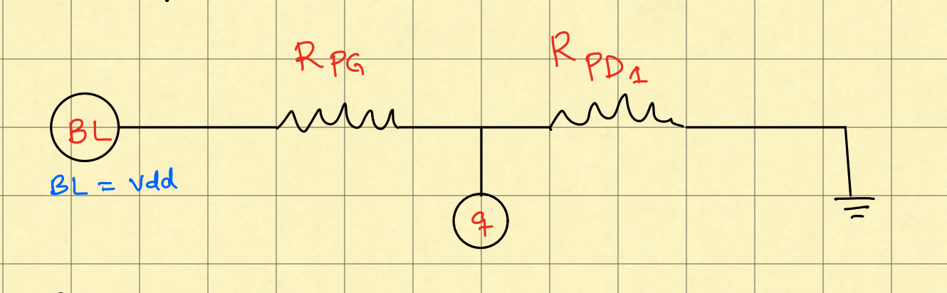
Assume the cell stores Q=0 and QB≈VDD. WL is high, and both bitlines are precharged to VDD. The pass-gate sources current from BL into Q while the pull-down sinks it. The handwritten cell and divider sketches show this contention directly.
4.1. Voltage-divider estimate
At fixed nominal length, a simple resistance model gives:
At 0.8 V this predicts 0.400, 0.320 and 0.267 V for β=1, 1.5 and 2. These are hand estimates. The measured DC zero-node crossings are 0.134, 0.097 and 0.077 V; the resistor approximation overestimates them because MOS device resistance varies with voltage. It correctly predicts that stronger PD reduces the disturb.
4.2. MOS current balance
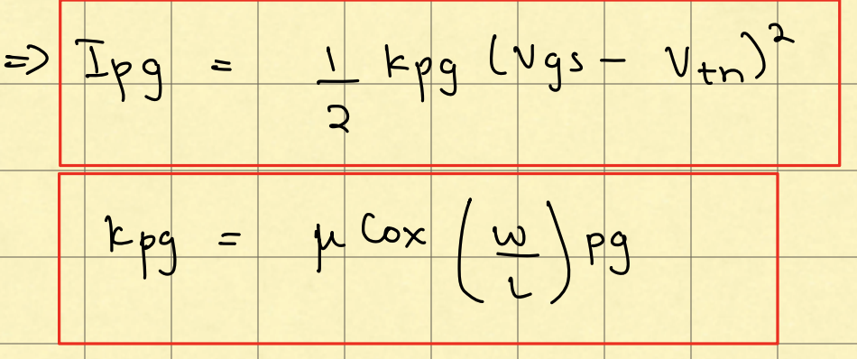
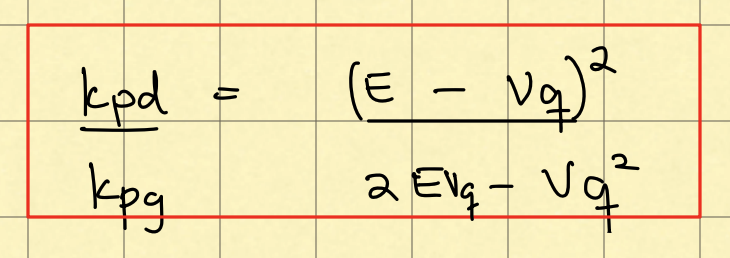
With \(E=V_{DD}-V_{Tn}\), the idealized saturated PG and triode PD currents are:
At DC equilibrium \(I_{PG}=I_{PD}\). The physical root is \(V_Q=E(1-\sqrt{\beta/(1+\beta)})\). This long-channel model assumes equal NMOS thresholds, negligible body effect and the stated operating regions. It is a guide to the trend, not a substitute for GPDK simulation.
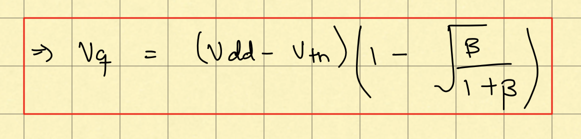
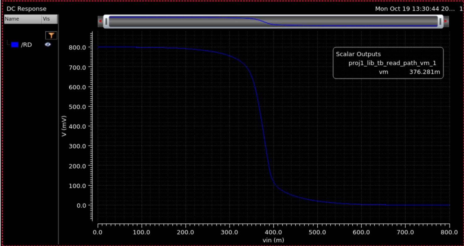
The disturbed Q node drives the opposite inverter. Read stability requires \(V_Q<V_M\), where \(V_M\) is that inverter’s switching point. In a square-law approximation, \(V_M=(V_{Tn}+B(V_{DD}-|V_{Tp}|))/(1+B)\) with \(B\approx\sqrt{\gamma\mu_p/(\beta\mu_n)}\). Since \(V_M\) was not separately measured, the actual read-margin comparison is the butterfly result.
5. Write-stability hand analysis
To overwrite a stored one with zero, start with Q≈VDD and QB≈0, assert WL, and drive the write-zero bitline to ground. The access transistor discharges Q against the ON pull-up. A first-order divider gives:
A smaller γ lowers the written node. The cell flips only if Q falls below the receiving inverter’s switching point, so the estimate requires \(V_Q<V_M\). With \(\rho=\mu_n/\mu_p\), the divider implies \(\gamma<\rho V_M/(V_{DD}-V_M)\). This is a conditional design inequality; it cannot prove a write margin without model strengths and a measured trip point.
5.1. Current-balance refinement
The original detailed write analysis treats the pass-gate as triode and the pull-up as saturated while \(V_Q<|V_{Tp}|\). Let \(E=V_{DD}-V_{Tn}\) and \(F=V_{DD}-|V_{Tp}|\). Equating the two branch currents yields:
The other quadratic root conflicts with the assumed pass-gate region; this expression also ceases to apply when PU enters triode. The completed manuscript retains the full typed derivation. No separate handwritten write image is present in media/part1/, so the site does not invent one.
The β=2, γ=1 candidate still needs the handout’s write-margin sweep: store Q=1, hold the opposing bitline high, sweep the write-zero bitline down from VDD, and record its flip voltage. A stronger PG can improve write ability but weaken read stability and increase bitline load; the read sweep alone cannot close that trade-off.
6. Read-SNM experiment and evidence
6.1. Actual testbenches
For each β, the read bench holds WL, BL and BLB at VDD=0.8 V. One DC bench sweeps Q and records QB; the other sweeps QB and records Q with feedback broken. The two original Virtuoso testbench captures below document the biasing and signals used.
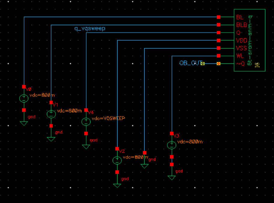
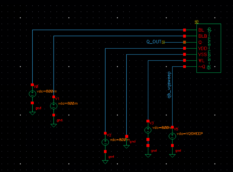
The four-column ViVA raw.csv for each β is split into q.csv and qb.csv; one curve is reflected about \(y=x\). scripts/check_snm_sweep.py finds the three intersections and fits the largest voltage square in each butterfly lobe. The smaller lobe side is \(SNM_{read}\). Its final 16,001-point computation differs from a 4,001-point check by at most 0.05 mV.
| β | PD fins | SNM left/right | Read SNM | Low crossing |
|---|---|---|---|---|
1.0 |
2 |
126.6 / 126.6 mV |
126.6 mV |
134.3 mV |
1.5 |
3 |
145.8 / 145.8 mV |
145.8 mV |
96.6 mV |
2.0 |
4 |
156.3 / 156.3 mV |
156.3 mV |
77.1 mV |
At the handout’s two-significant-figure precision, read SNM is 0.13, 0.15 and 0.16 V; the disturbed zero-node crossings are 0.13, 0.097 and 0.077 V. The table retains extra digits to trace the calculations.
The low-voltage crossing is the reported DC zero-node read-disturb operating point. The β=2 schematic improves read SNM by 29.7 mV (23%) over β=1 at 0.8 V, while lowering that crossing by 57.2 mV.
6.2. Original ViVA butterflies with measured-square overlays
These are the original Cadence screenshots. Cyan outlines are drawn by this report/site at the square positions stored in each snm.json. The ViVA x and y axes have unequal pixel scales, so a square in volts appears rectangular on the screenshot. The outlines are computed annotations, not an indication that Cadence directly reported SNM. All three captures preserve the original trace colors and axes.
On a phone, swipe the captures sideways to inspect the full axes and overlays.
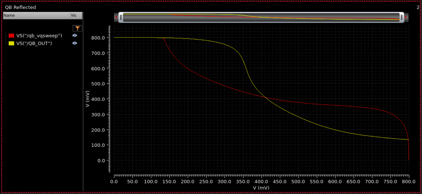
beta1/snm.json; smaller fitted side 126.6 mV.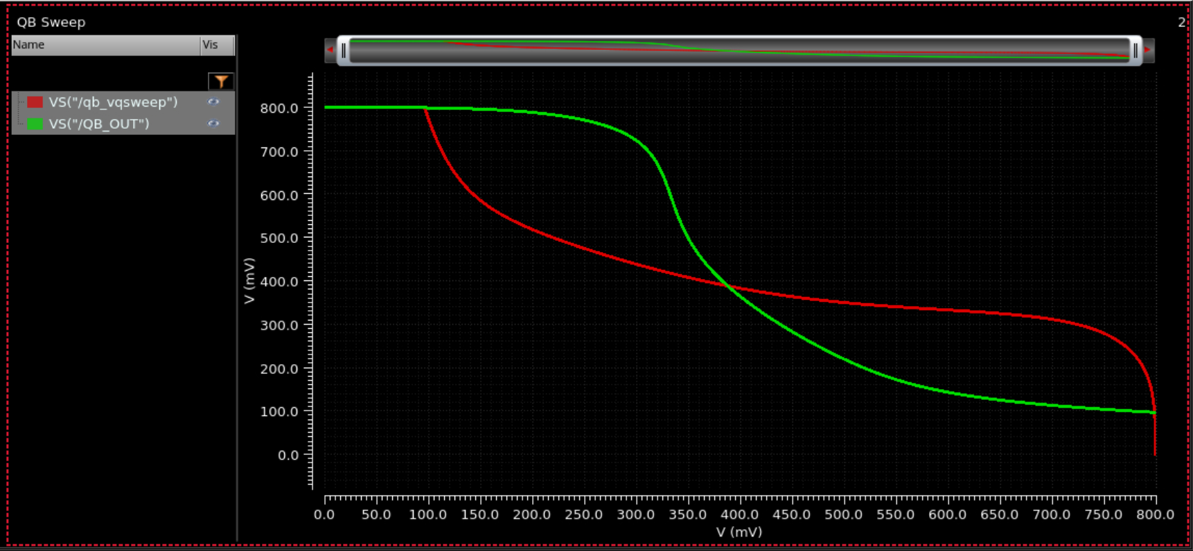
beta1p5/snm.json; smaller fitted side 145.8 mV.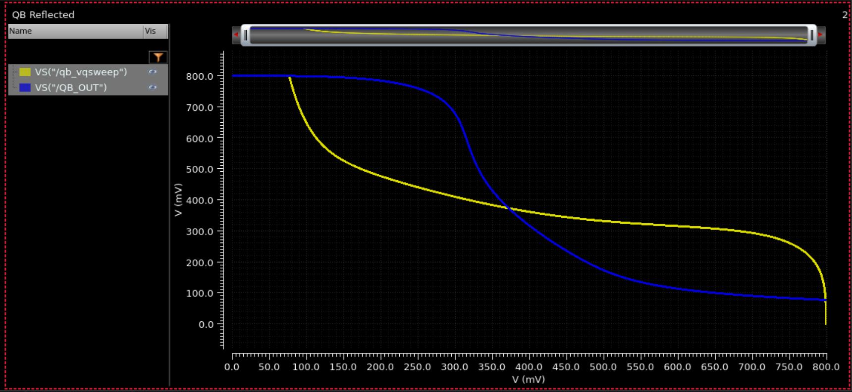
beta2/snm.json; smaller fitted side 156.3 mV.6.3. Data trail
results/part1/read-snm/beta*/raw.csv is the verbatim ViVA export. The normalized q.csv and qb.csv, computed snm.json and clean butterfly PNG/SVG are reproducible derivatives. Run:
python3 scripts/check_snm_sweep.py --allThe clean plots are secondary reading aids; the screenshots above are the original Cadence view. This sweep is schematic. The extracted read SNM that supersedes 156.3 mV is 140 mV, in post-layout stability.
7. Layout, extraction and post-layout results
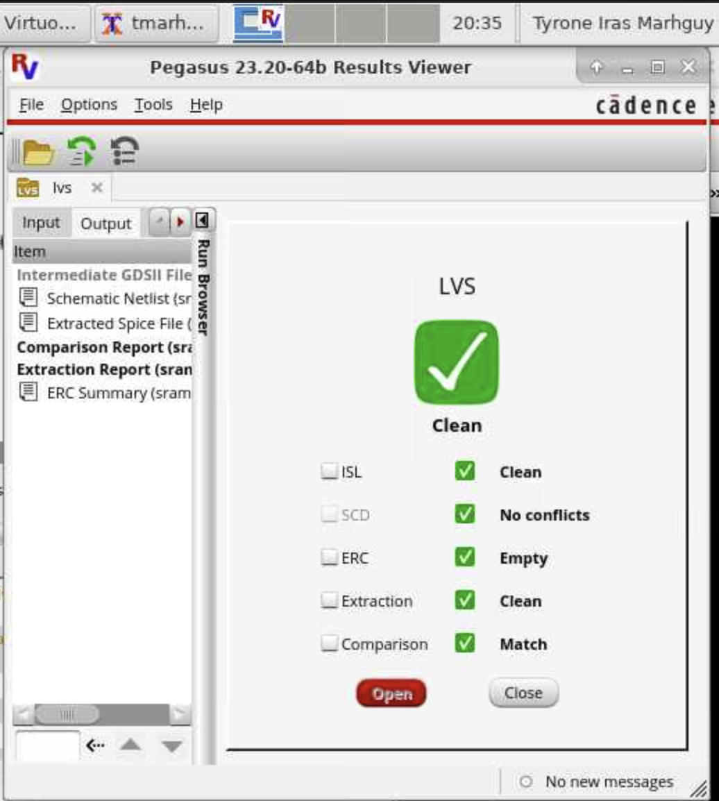
The numbers below are the same ones in the PDF. DRC and LVS are pass/fail: a clean cell is 0 violations and a match, not a partial marker count.
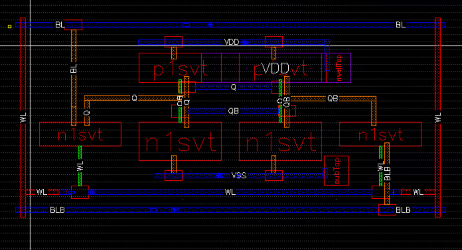
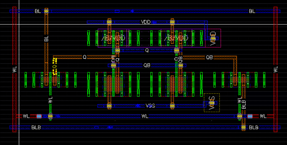
7.1. Floorplan
The drawn cell keeps the schematic sizes: L=18 nm, pull-ups at 2 fins, pull-downs at 4 fins, pass-gates at 2 fins.
-
Two pull-ups in the top row, each contacted to a horizontal VDD rail.
-
Two pull-downs in the bottom row, tied by a horizontal VSS rail.
-
\(Q\) and \(\overline Q\) running horizontally between the cross-coupled devices.
-
WL along the bottom edge and up both sides of the cell.
Mirrored neighbours can share the VDD rail, the VSS rail, and the bitline contacts. The PR boundary is 0.72 µm by 0.54 µm.
| Quantity | Value | Source |
|---|---|---|
Pegasus DRC |
0 violations |
|
Pegasus LVS vs. |
Clean, comparison match |
|
Cell width × height |
0.72 × 0.54 µm |
PR boundary. Width is the bitline pitch; height is the wordline pitch. |
Cell area |
0.39 µm² = 3900 \(F^2\) |
0.72 × 0.54 |
Density factor \(D\) |
28 |
\(A_{\mathrm{cell}} / \sum W_i L_i\) |
The area is the PR-boundary area that abutting cells repeat. It includes the half-rails and half-bitline contacts shared with mirrored neighbours.
7.2. Density factor
The handout estimates un-laid-out blocks as \(A_{\mathrm{est}}=D\sum_i W_i L_i\), with \(D\) measured on this cell. One fin counts as the PDK fin pitch, \(W_{\mathrm{fin}}=48\,\mathrm{nm}\), and \(L=18\,\mathrm{nm}\) on every device. The cell has 16 fins, so
The same fin-pitch convention has to be used for every \(\sum W_i L_i\) in Parts 2 and 3.
7.3. Extraction
Parasitics come from the layout with the tutorial Quantus flow (C+CC).
| Node | Capacitance | Meaning for Part 2 |
|---|---|---|
BL (one bitline, one cell) |
180 aF |
\(C_{BL} \approx 16\times 180\) aF, plus wire, per column |
WL (one cell) |
90 aF |
\(C_{WL} \approx 4\times 90\) aF, plus wire, per row |
The bitline term is the pass-gate drain junction plus the shared bitline contact. The wordline term is two pass-gate gates plus the WL wire across the cell. Fifteen copies of 180 aF are the stand-in column load in the functional check.
7.4. Post-layout stability at 0.8 V
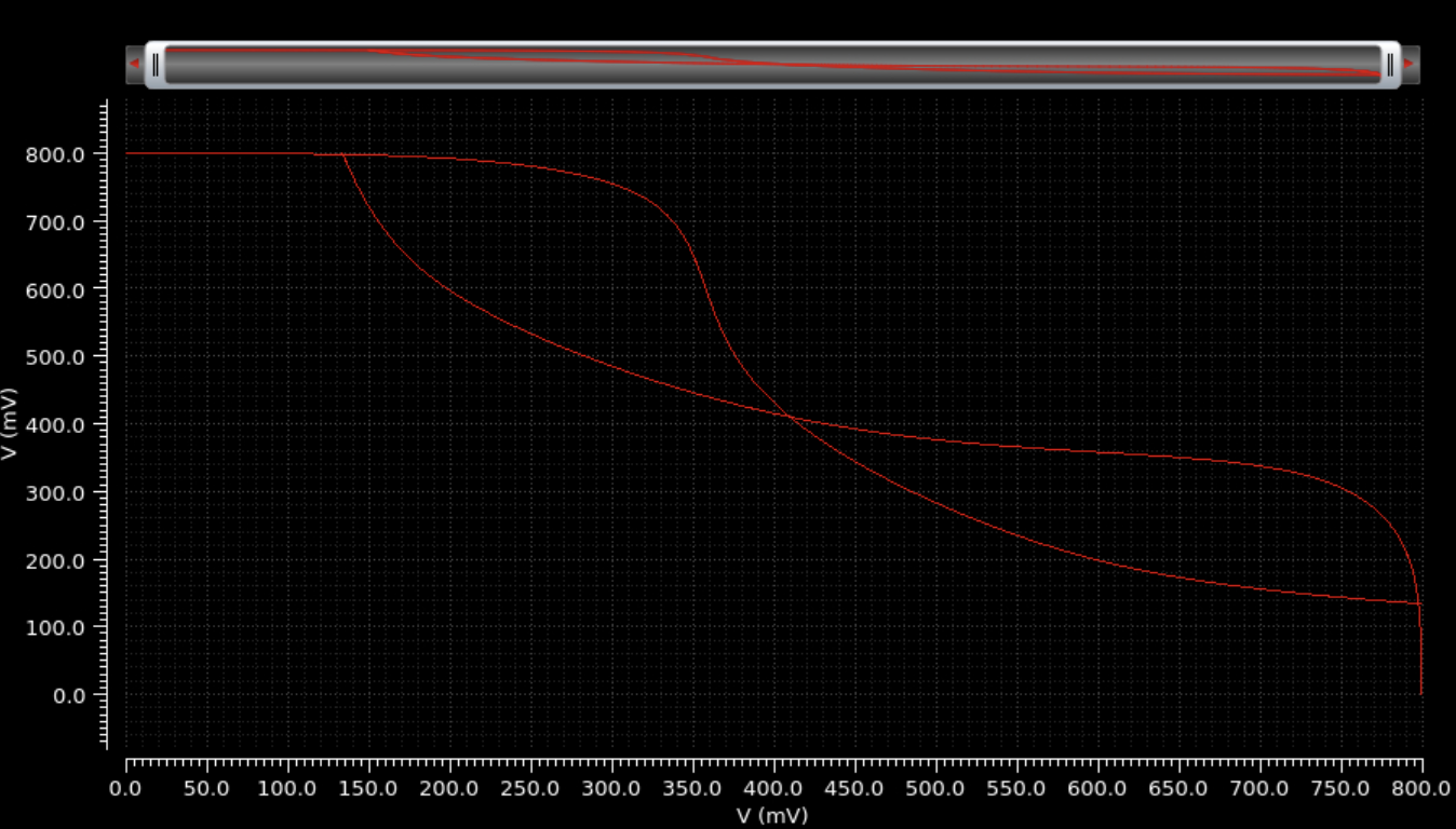
These benches use the extracted view. The margin is the same largest-square reduction as the schematic sweep. If the butterfly is asymmetric, SNM is the smaller side.
| Item | Bench | Result |
|---|---|---|
Hold SNM |
WL=0; feedback broken; both VTCs overlaid |
280 mV |
Read SNM |
WL=\(V_{DD}\), BL=BLB=\(V_{DD}\) |
140 mV |
Read "0" node |
DC voltage of the disturbed zero node; schematic crossing was 77.1 mV |
95 mV |
Write margin |
Store Q=1; WL=\(V_{DD}\); BLB held at \(V_{DD}\); sweep BL from \(V_{DD}\) to 0 |
0.42 V |
Cell current |
Both bitlines at \(V_{DD}\); current from the zero-side bitline |
25 µA |
Extraction lowers read SNM from the schematic 156.3 mV to 140 mV and raises the disturbed zero node from 77.1 mV to 95 mV. Hold SNM, 280 mV, stays well above the read margin.
| \(V_{DD}\) (V) | SNMread (mV) | \(\mathrm{WM}_{BL}\) (V) | Comment |
|---|---|---|---|
0.8 |
140 |
0.42 |
nominal; supersedes the 156.3 mV schematic result |
0.7 |
110 |
0.32 |
|
0.5 |
70 |
0.18 |
still reads; write is the weak one |
Read SNM falls from 140 mV to 110 mV to 70 mV as the supply drops. \(\mathrm{WM}_{BL}\) falls from 0.42 V to 0.32 V to 0.18 V. At 0.5 V the cell still reads. The write is the weak result: 0.18 V is still a trip point, and it is the smallest margin in the table.
7.5. Functional check
The transient bench drives WL and the precharge devices with ideal pulses and loads each bitline with the extracted cell plus 15 copies of 180 aF, standing in for a 16-row column. The sequence is write 0, read, write 1, read. The capture (media/part1/functional_check.png) is not in the repository yet.
7.6. What limits the cell
Read stability is set by the pass-gate/pull-down divider. The schematic sweep moved the disturbed zero node from 134 mV (β=1) to 77 mV (β=2). Extraction gives 140 mV of read SNM and a 95 mV zero node at 0.8 V, against a hold SNM of 280 mV, so the read is what the Part 2 noise budget has to clear. The four-fin pull-down sets the 0.54 µm cell height and most of \(C_{WL}=90\) aF. The two-fin pass-gate sets \(C_{BL}=180\) aF and the 25 µA read current. Writability is the γ=1 limit: \(\mathrm{WM}_{BL}\) is 0.42 V at 0.8 V and 0.18 V at 0.5 V. The cell still reads at 0.5 V (70 mV). The write is the weak one, so a Part 2 remedy, if that margin is not enough for the column, is a weaker pull-up or a write assist rather than a new cell. Part 2 keeps this cell, mirrors it to share the BL contacts and the VDD/VSS rails, and sizes the wordline driver and precharge from 16 × 180 aF and 4 × 90 aF plus wire.
7.7. Team contributions
Both authors are responsible for the complete design and report.
| Author | Contribution |
|---|---|
Tyrone Marhguy |
Part 1 6T cell: schematic, β sweep, pull-up/pass/pull-down sizing, custom layout, DRC and LVS. Part 2 SRAM macro, instantiated twice as W and X. Part 3 |
Victor Wanjohi |
Part 1 write-stability analysis. Part 2 column circuits, decoder, and SRAM-macro benches (\(T_{CLK}\), power, access). Part 3 leaf cells ( |
8. SRAM macro (Part 2)
The Part 1 cell is tiled into a 16×4 synchronous SRAM (sram_macro) with a 4-to-16 predecoder, per-column precharge, write driver, 2:2 read path and output latch, and a delay-chain controller. Wordlines run horizontally; bitline pairs run vertically. The 64 cells keep the Part 1 sizes (no one-off resize). Bitline stand-in load is \(C_{BL}=3.5\) fF (cbw plus 16 × 180 aF). Simulations in this chapter are schematic-level. Area uses \(D=28\) from Part 1 except the array, which is 64 × 0.389 µm².
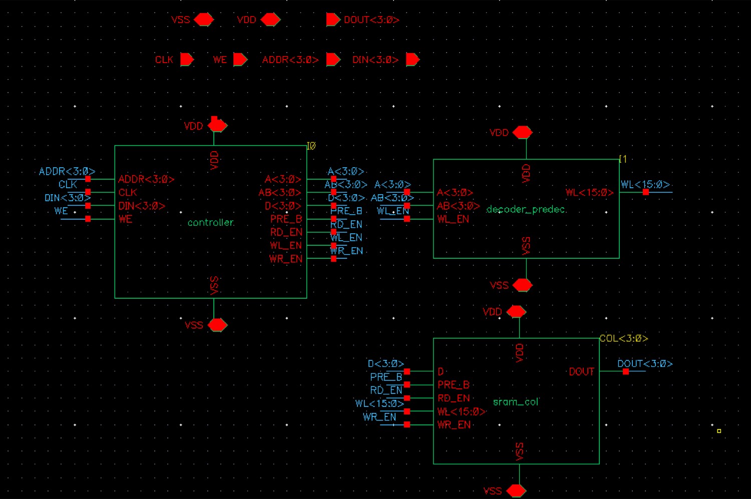
sram_macro schematic| Quantity | Value | Notes |
|---|---|---|
Array (64 cells) |
24.9 µm² |
tiled from the Part 1 PR boundary, not a new layout |
Periphery |
29.7 µm² |
decoder 12.6 + controller 10.3 + columns |
Macro total |
54.6 µm² |
1226 periphery fins × 0.0242 µm² + array |
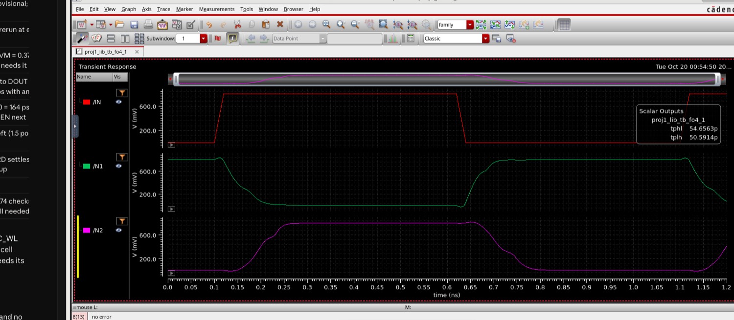
FO4 ( |
53 ps |
|
\(T_{CLK}\) |
0.69 ns |
shortest passing period on |
\(t_{\mathrm{acc}}\) fall / rise |
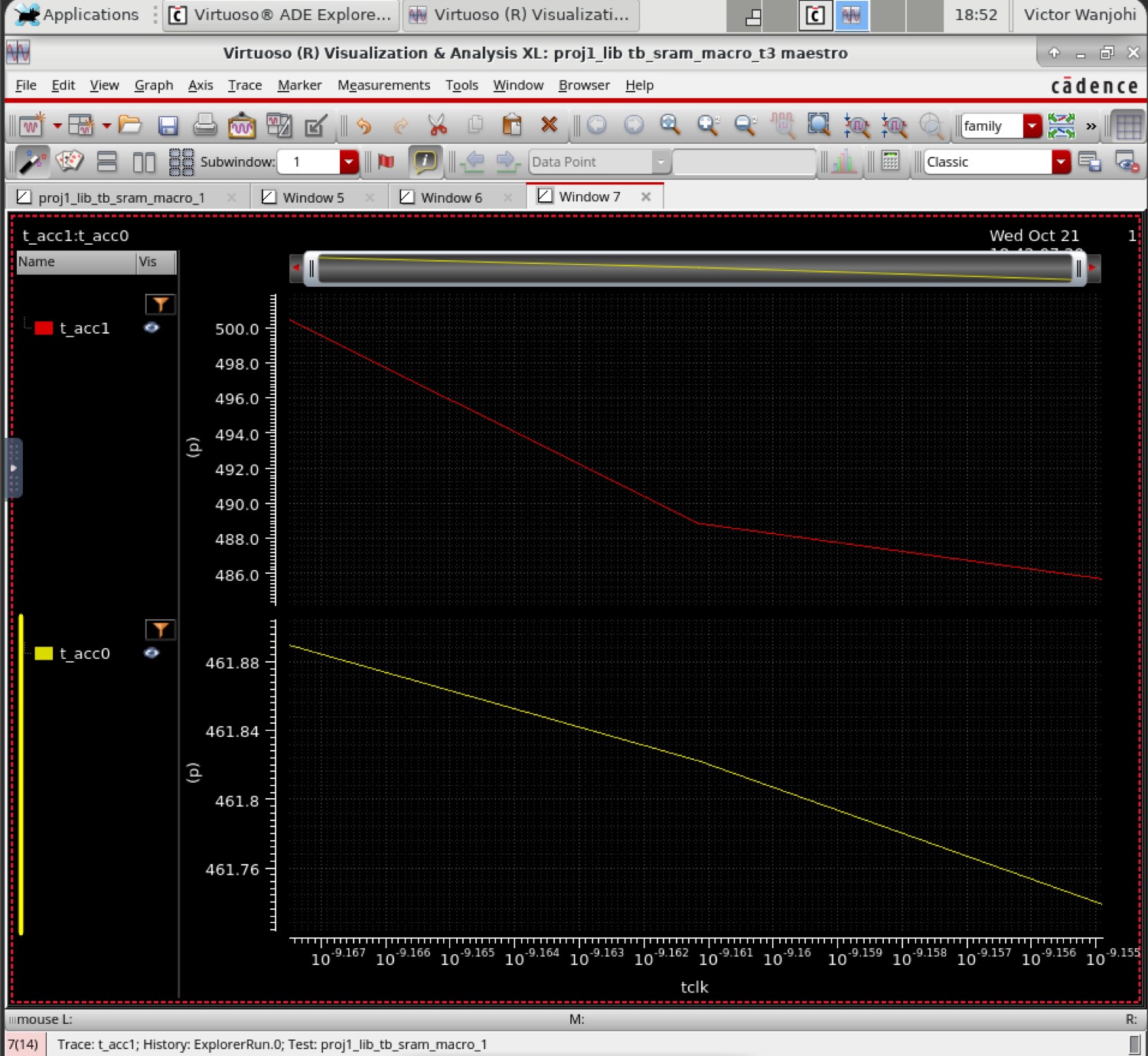
463.7 / 484.2 ps |
1 ns bench, DOUT⟨1⟩ at addresses 0 and 1 |
\(t_{\mathrm{access}}\) (worst) |
488 ps |
CLK to DOUT, read of 1 at 0.69 ns |
err1 / err2 / err3 |
173.8 µV (pass) |
spec 0.1 V |
\(P_{\mathrm{read}}\) |
115.2 µW |
checkerboard at 0.69 ns |
\(P_{\mathrm{leak}}\) |
3.99 µW |
clock stopped |
FOM |
\(\approx 4.7\times10^{3}\) |
Area × write power × \(T_{CLK}\) |
Part 2 PDF has the full benches, decoder logical-effort write-up, and power tables.
8.1. Periphery
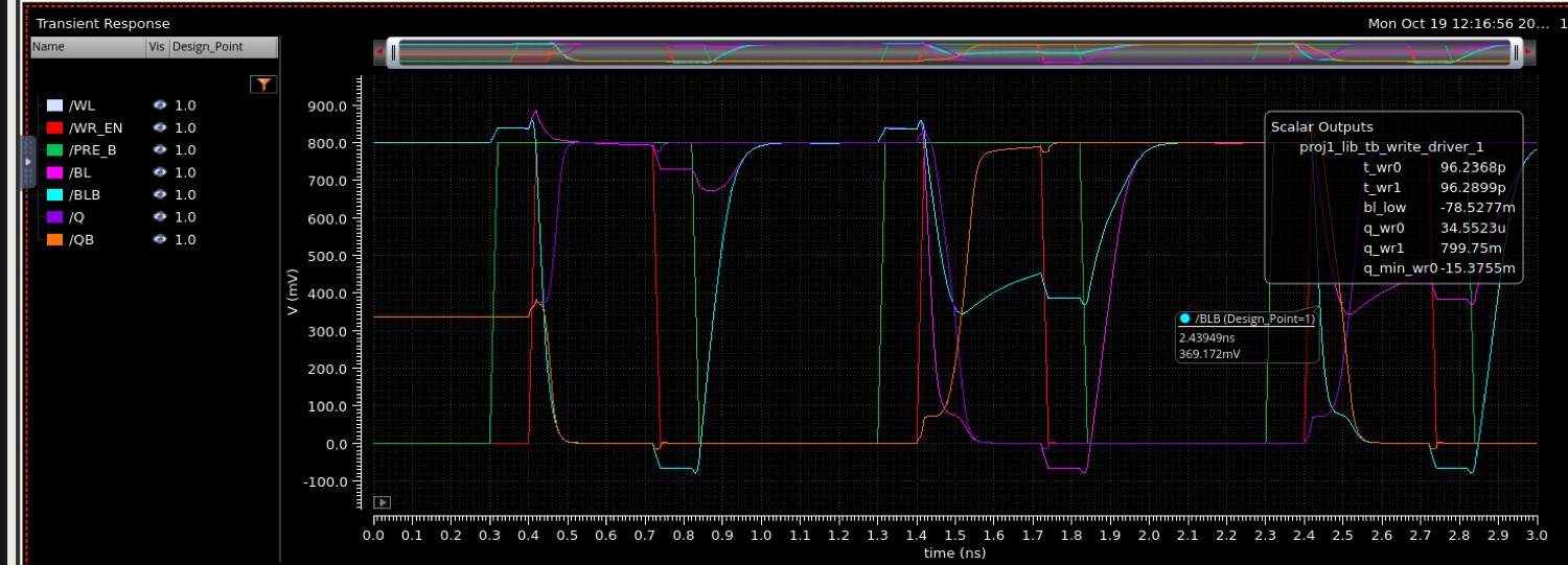
Write driver NMOS stacks are nfin=8 (smallest that writes at 3.5 fF is nfin=5; nfin=8 writes in 96 ps with BLB staying above ~0.34 V). Minimum write pulse at 50% is 100–120 ps; design pulse ~140 ps.
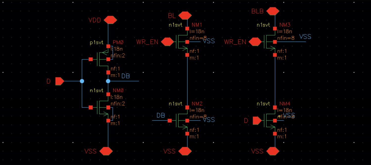
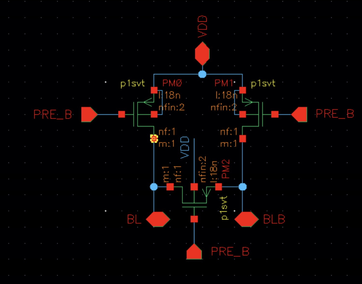
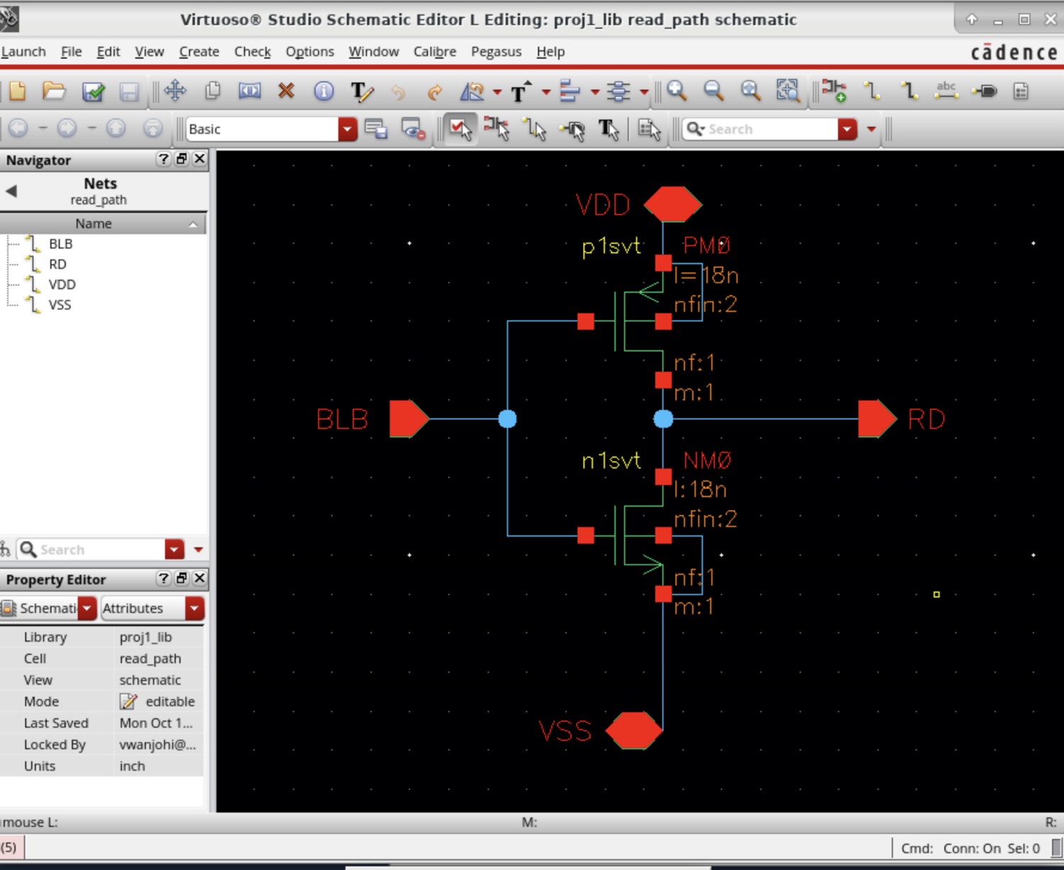
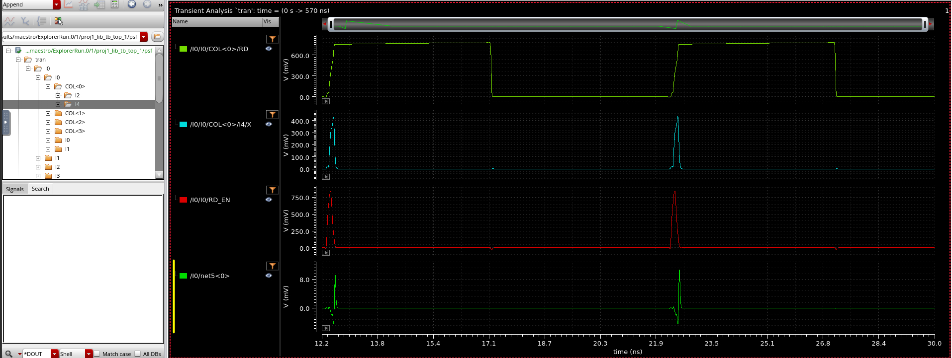
Precharge is three 2-fin PMOS per column. Read path is a 2:2 inverter into an output latch enabled on the clock-high phase (see Part 3 for the RD_EN fix on tb_top).
8.2. Decoder
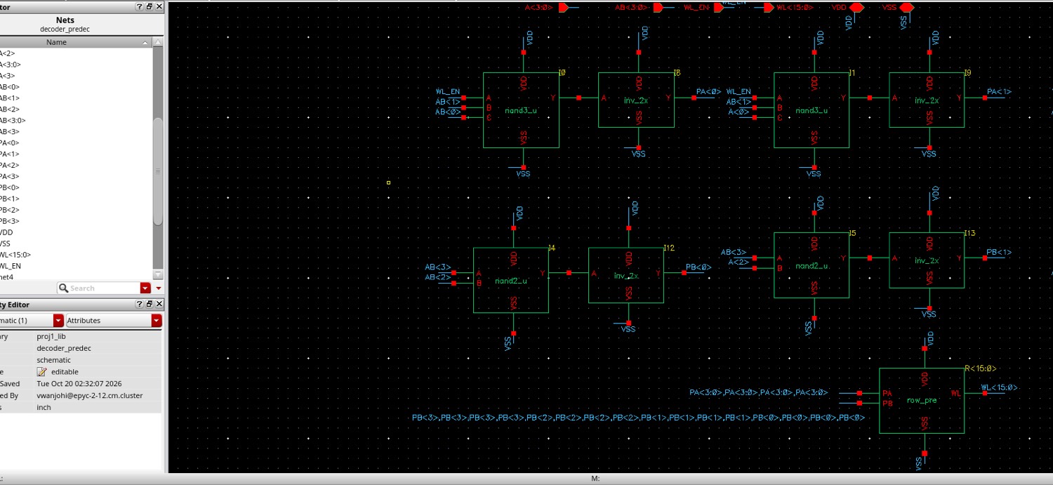
Chosen decoder is a 2–2 predecode (NAND3 + inv_2x + row NAND2 + inv_drv). Logical effort with B=8 (address fan-out) predicts 182 ps address-to-wordline (\(\tau=10.5\) ps from FO4=53 ps). Measured A⟨0⟩ path: 106 ps (new row rising) / 112 ps (old row falling).
8.3. Full-macro bench
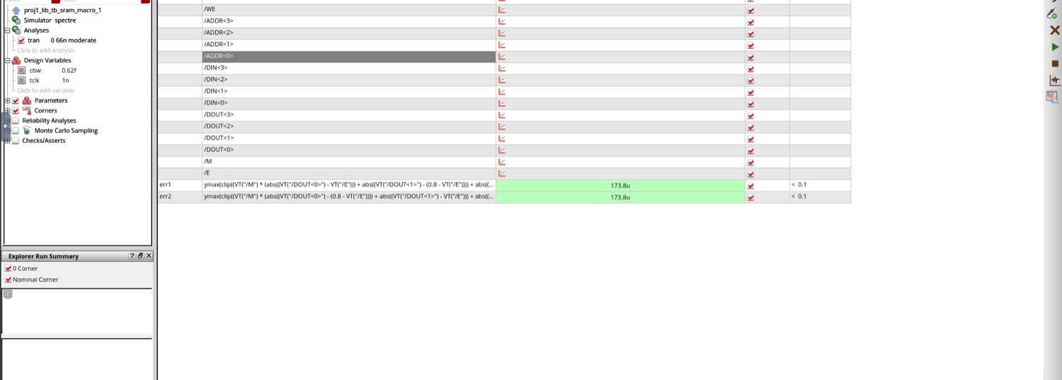
tb_sram_macro writes 16 words, reads them, writes the complement, and reads again. err1 / err2 / err3 (M-weighted DOUT error) all pass at 173.8 µV against a 0.1 V spec. Worst-case access at \(T_{CLK}=0.69\) ns is 488 ps on a read of 1.
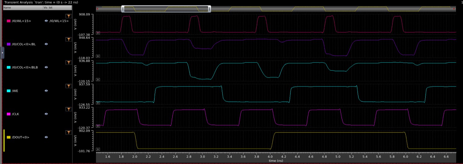
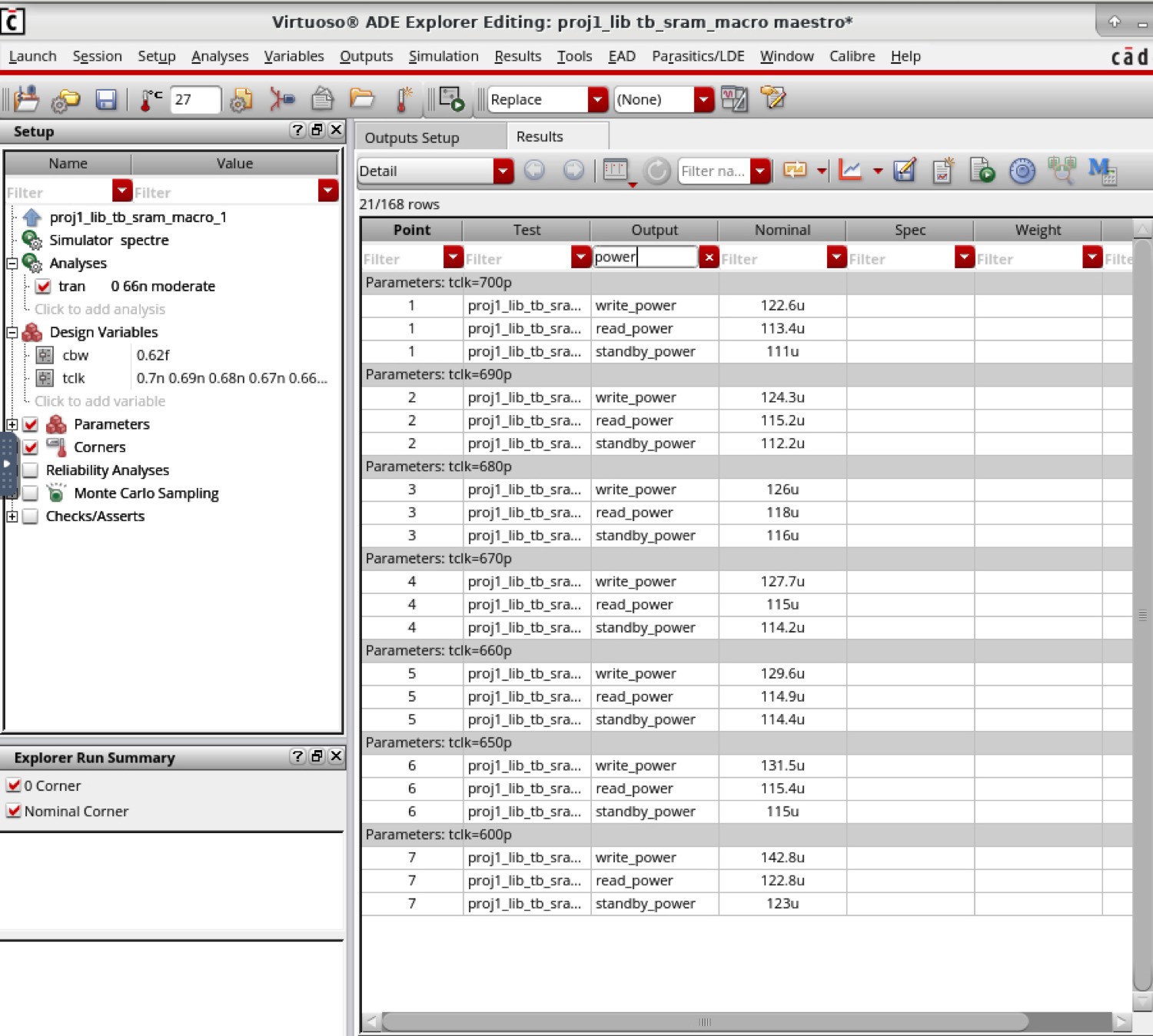
Clock-running idle (112.2 µW) is almost the read power (115.2 µW): the delay-chain controller has no chip-select, so SRAM energy in Part 3 is nearly pattern-independent.
9. MAC unit (Part 3)
Two Part 2 macros hold W and X. A static-CMOS array multiplier, a 12-bit ripple accumulator, a 4-bit counter and controller_mac compute the dot product. The macro output latch is the only pipeline stage: SRAM access and arithmetic share one period. Tests A, B and C all pass at 10, 4.0 and 2.5 ns. At 2.0 ns, A finishes at 0x34D and C at 0x320 (pass) while B finishes at 0xC10 instead of 0xE10 (fail). At 1.75 ns and 1.5 ns all three fail. Selected \(T_{CLK}=2.5\) ns (400 MHz), \(t_{dot}=17\times2.5=42.5\) ns. Energy and FOM use that same period. All of this chapter is schematic-level.
Part 3 PDF is the Gradescope write-up (figures, DFF tables, energy integrals).
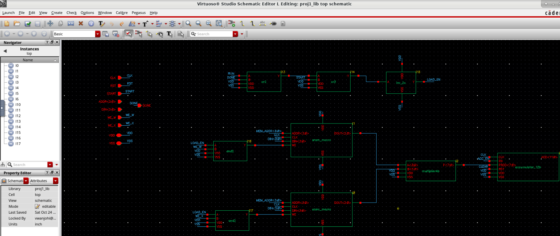
top, left half: SRAM macros I1/I0, multiplier, accumulator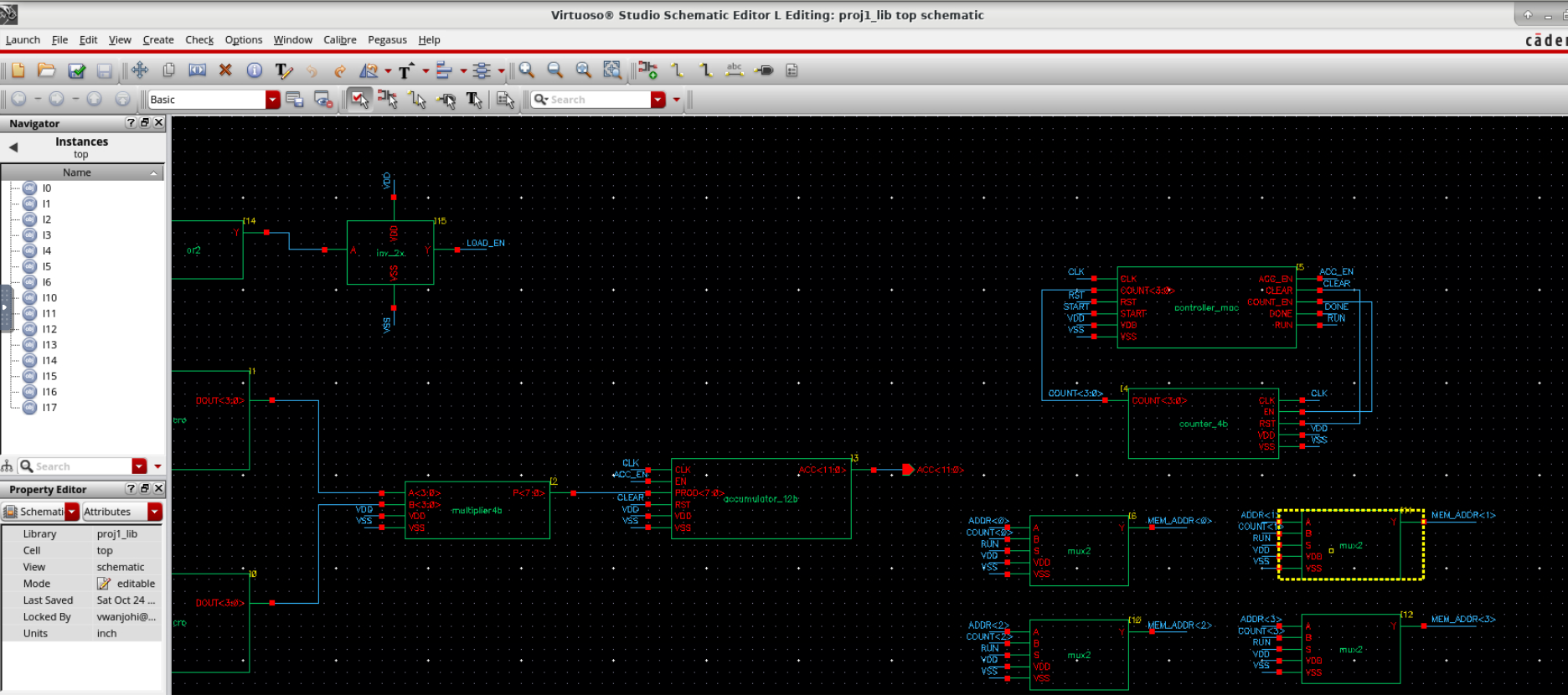
top, right half: controller, counter, address muxes| Metric | Value |
|---|---|
\(V_{DD}\) |
0.8 V (nominal, 27 °C) |
Density factor D |
28 (one fin = 0.0242 µm²) |
\(T_{CLK}\) |
2.5 ns (400 MHz) |
\(N_{cycles}\) START→DONE |
17 |
\(t_{dot}\) |
42.5 ns |
Area |
291.8 µm² (est.): 2×54.6 SRAM + 137.8 datapath + 44.7 sequencer |
Test A \(E_{dot}\) |
8.870 pJ (0.5544 pJ/MAC), measured on V0 |
Test A without memory |
0.38 pJ/MAC (est.) |
FOMMAC |
\(1.1\times10^{5}\) µm²·pJ·ns |
9.1. Register
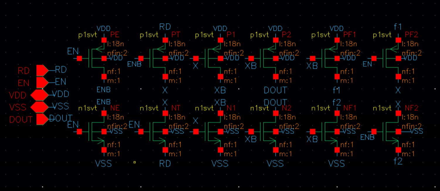
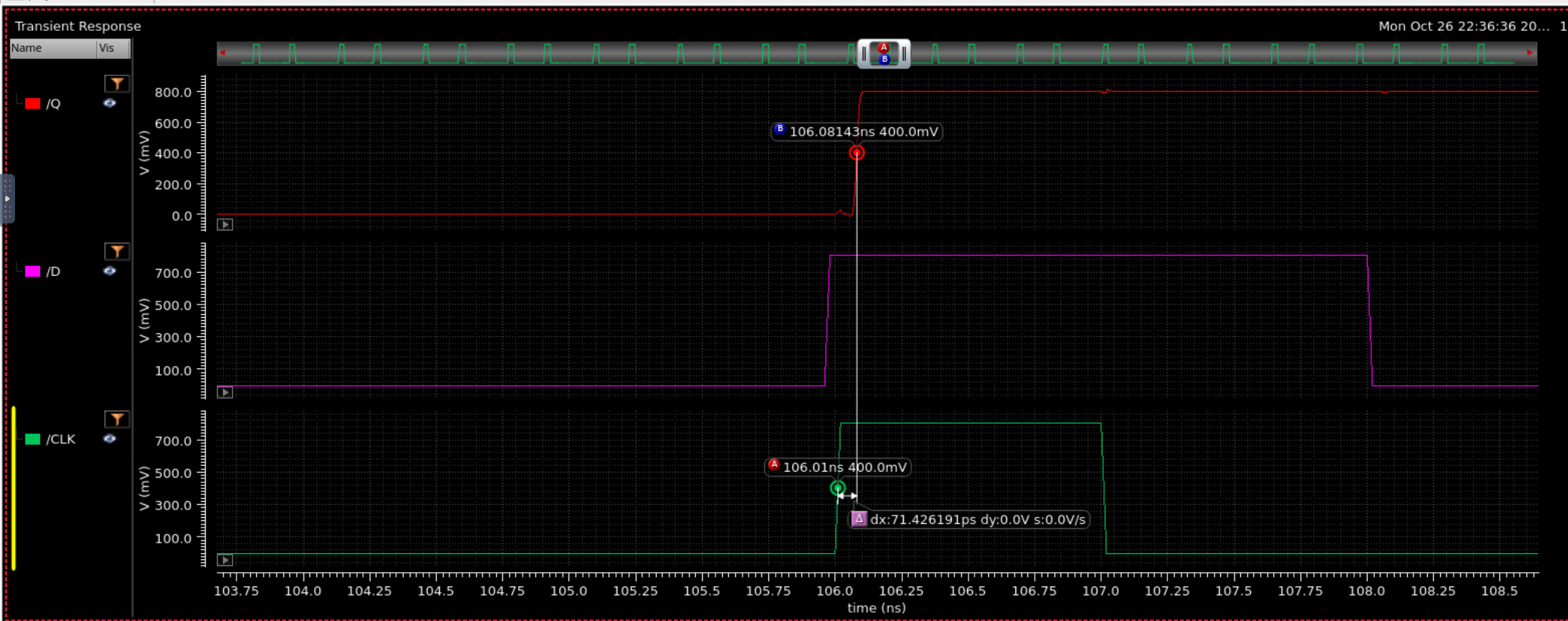
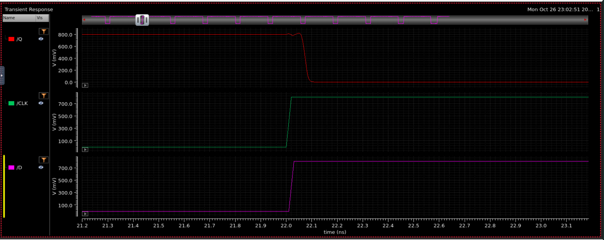
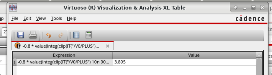
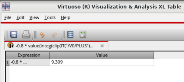
Positive-edge TG master-slave (d_ff), 100 fins, fully static so IDLE and DONE can stop the clock. \(C_Q=1\) fF, 0.4 V markers.
| Quantity | Value | Notes |
|---|---|---|
\(t_{cq}\) rise / fall |
68.51 / 62.18 ps |
CLK and Q at 0.4 V |
\(t_{su}\) both edges |
40 ps |
10% \(t_{cq}\) wall; 30 ps fails |
\(t_{h}\) rise / fall |
10 ps / ≤0 ps |
functional; 0 ps rise fails |
\(C_{CLK}\) |
2.822 fF |
rising-edge integral on |
Energy idle / toggle |
3.895 / 9.309 fJ |
20 clocks, 10–90 ns |
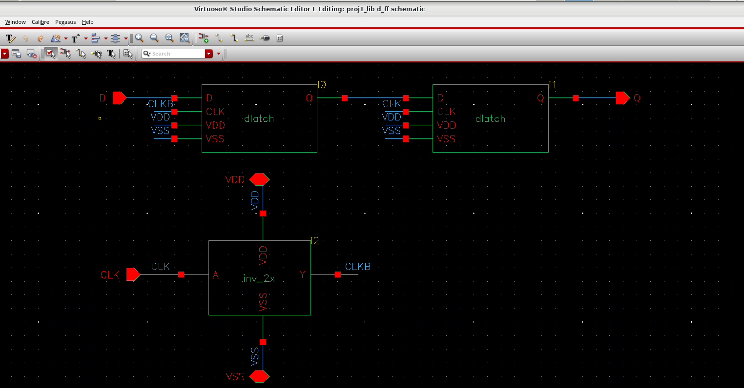
d_ff: master on CLKB, slave on CLK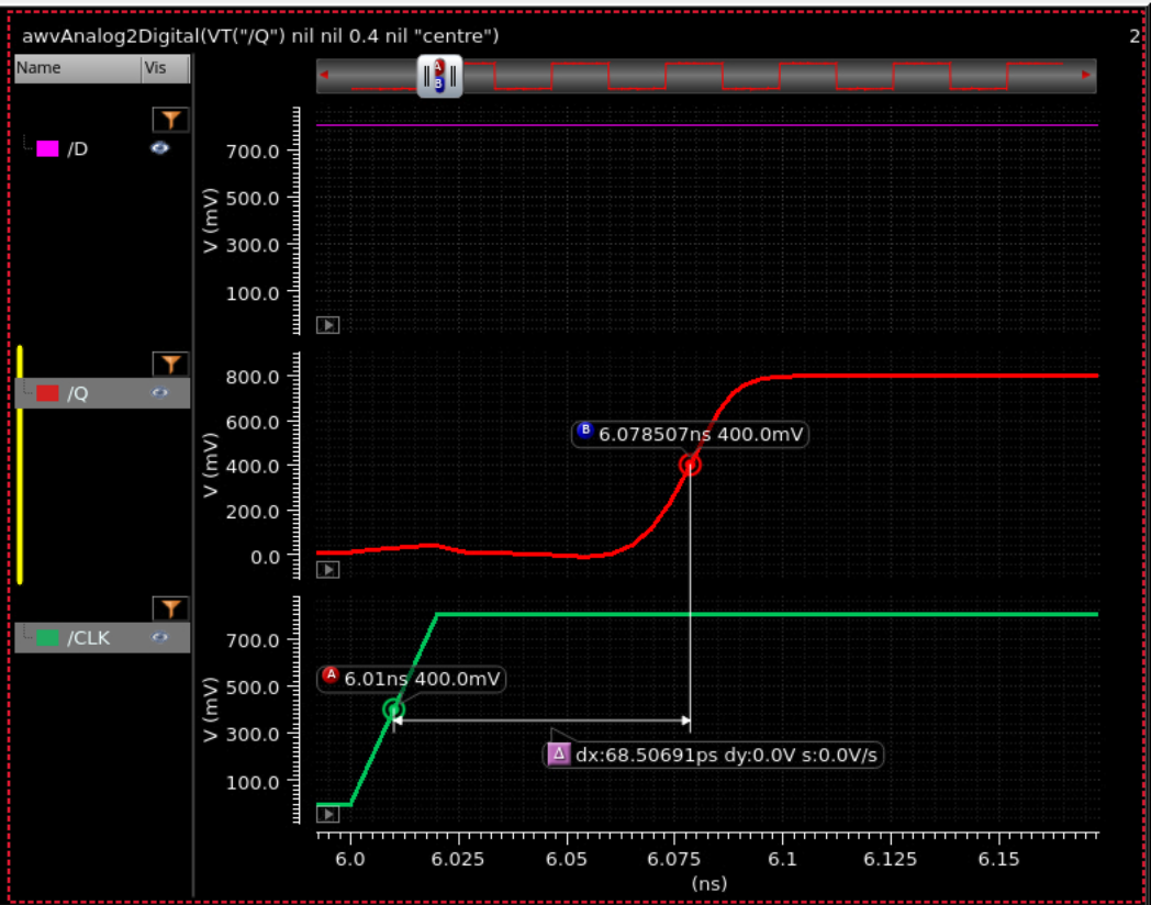
9.2. Datapath
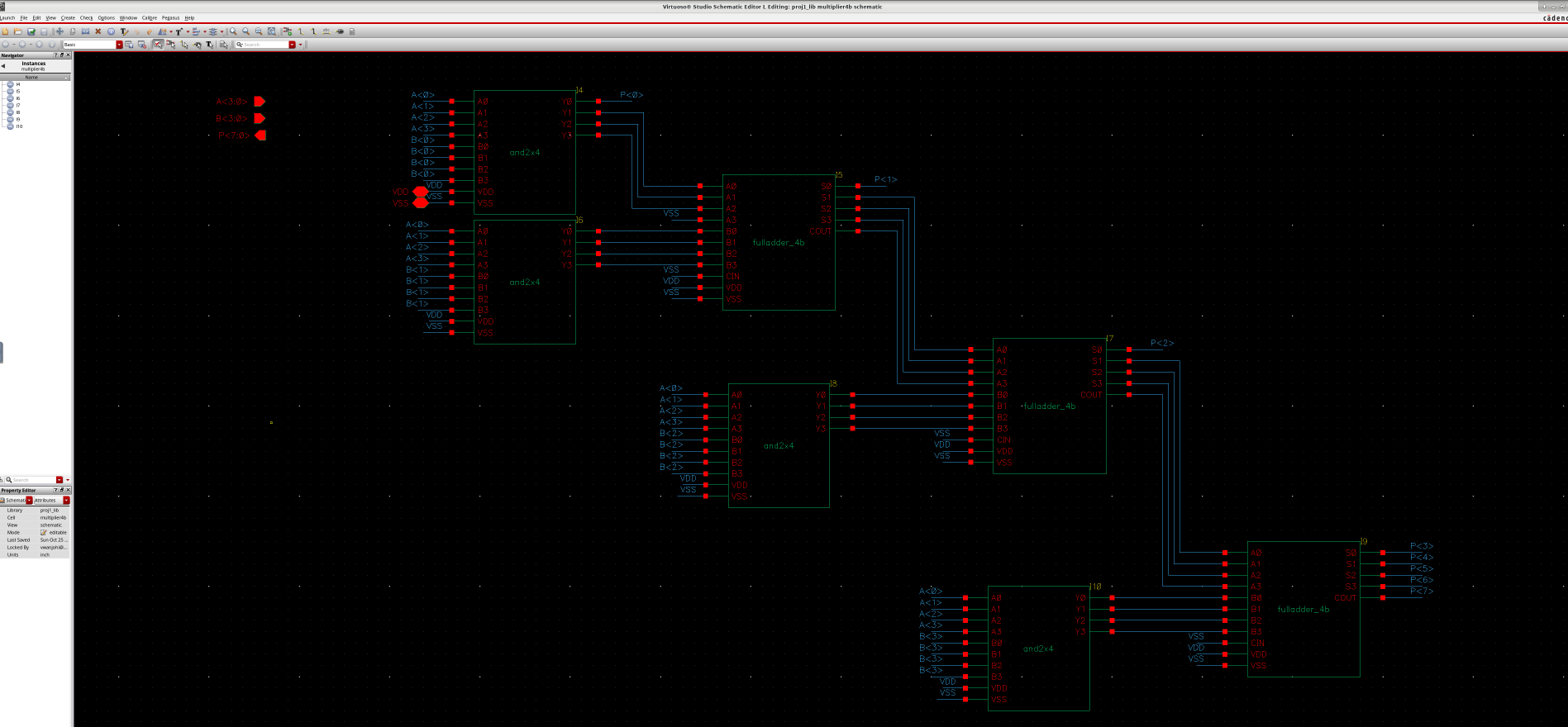
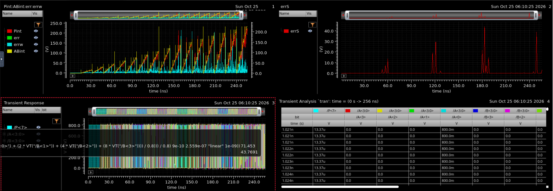
Leaf cells are static CMOS, L=18 nm. The 4×4 array multiplier is AND rows plus ripple full adders. Exhaustive 256/256 products match; measured worst case is 1.14–1.24 ns (vector 244, B=15). Hand logical effort is ~1.85 ns. The 12-bit ripple adder is twelve of the same full adder (148 fins each).
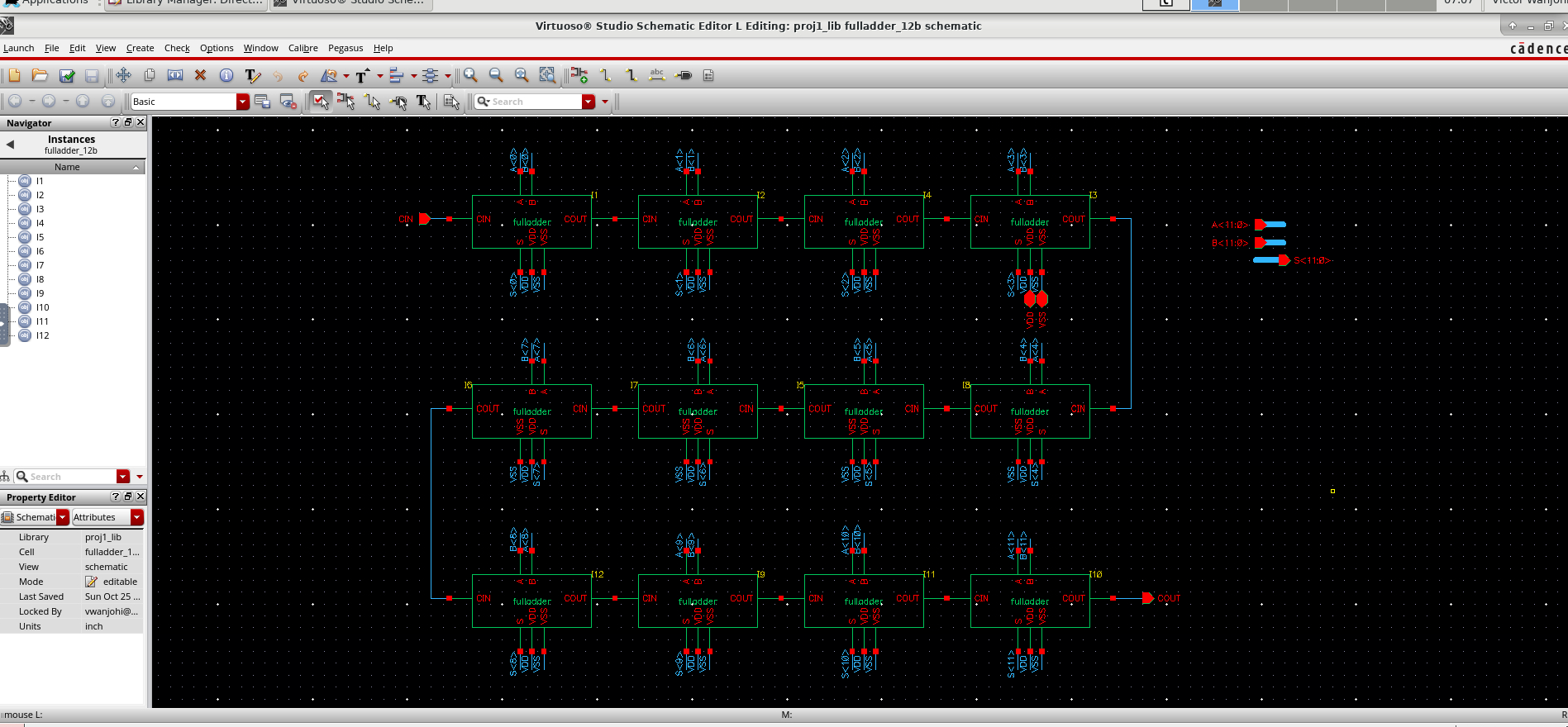
9.3. Sequencer
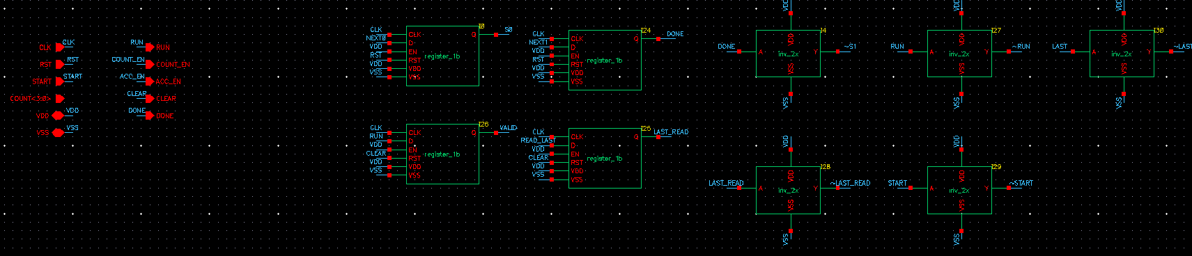
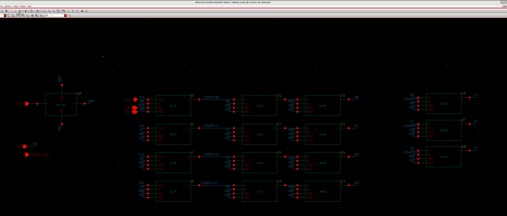
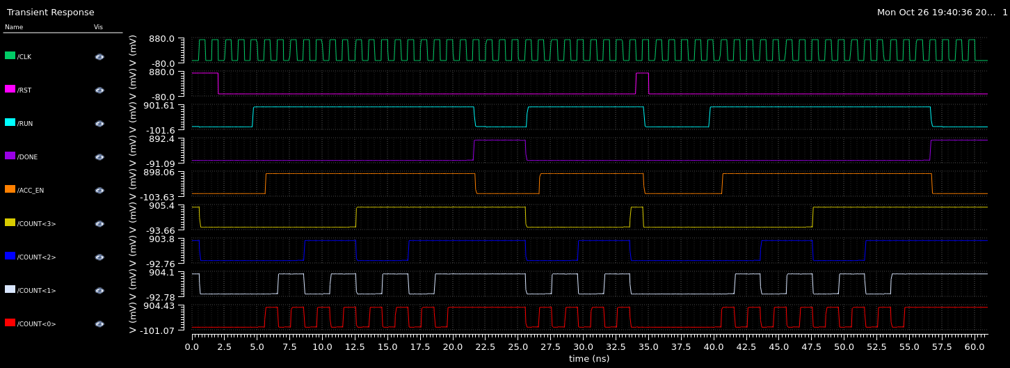
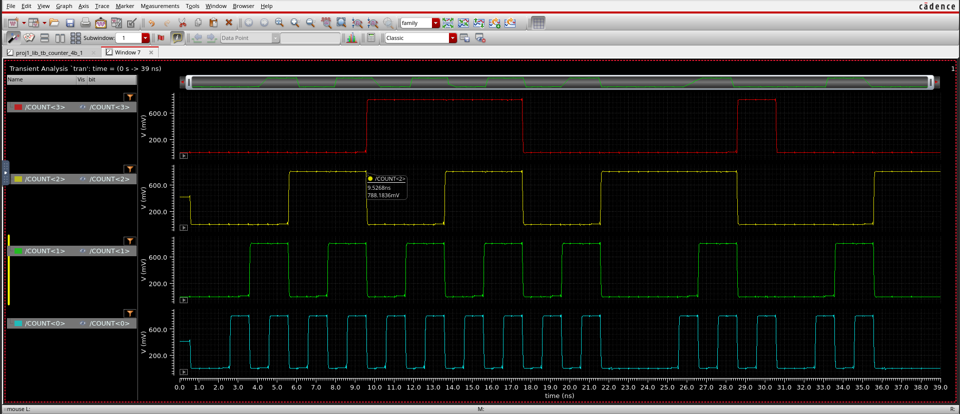
controller_mac plus counter_4b: START is sampled on a rising CLK; COUNT walks 0–15; both macros are read in cycles 0–15; VALID delays ACC_EN so accumulate occupies cycles 1–16; DONE rises on cycle 17. tb_controller_mac: 60/60 vector checks; tb_counter4b: 38/38.
9.4. Period sweep and Tests A/B/C
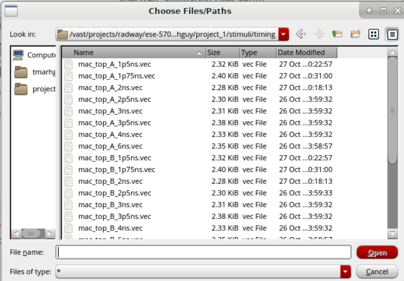
Expected finals: A = 0x34D (845), B = 0xE10 (3600, full-scale carries), C = 0x320 (800, 5/10 checkerboard). Vectors in stimuli/timing/mac_top_<A|B|C>_<period>.vec.
| \(T_{CLK}\) | Test A | Test B | Test C | Result |
|---|---|---|---|---|
10 ns |
0x34D, pass |
0xE10, pass |
0x320, pass |
pass |
4.0 ns |
0x34D, pass |
0xE10, pass |
0x320, pass |
pass |
2.5 ns |
0x34D, pass |
0xE10, pass |
0x320, pass |
selected |
2.0 ns |
0x34D, pass |
0xC10, fail |
0x320, pass |
fail (B) |
1.75 ns |
0x31D, fail |
fail |
fail |
fail |
1.5 ns |
0x13D, fail |
fail |
fail |
fail |
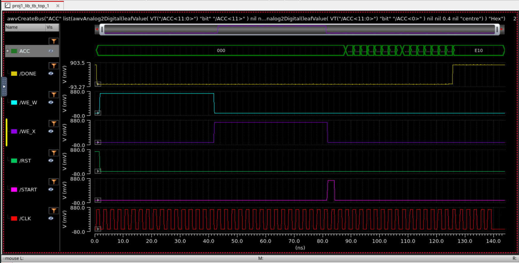
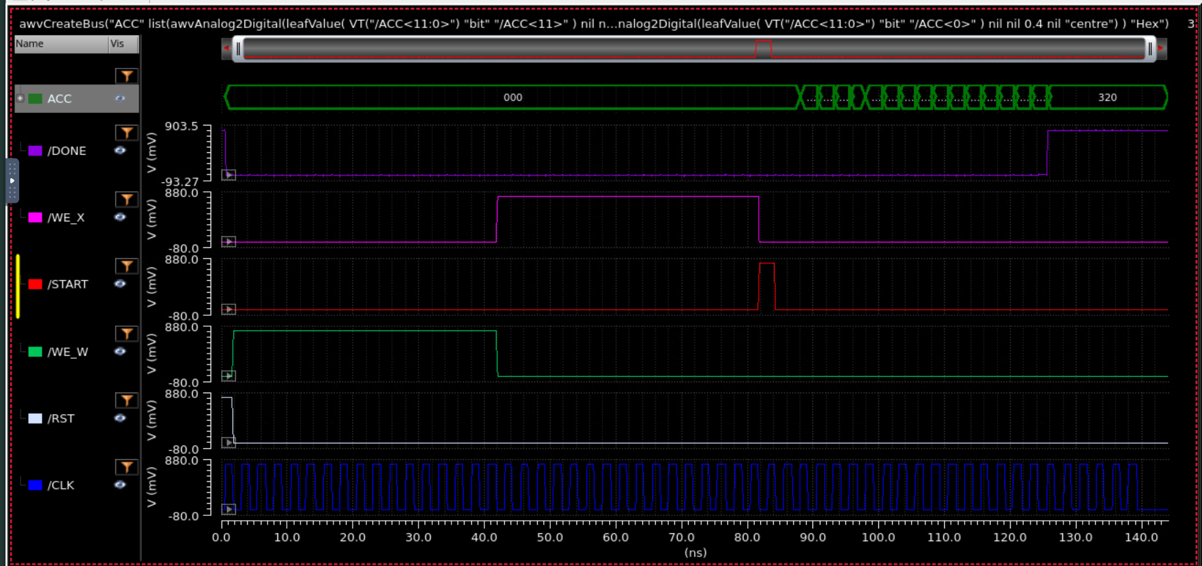
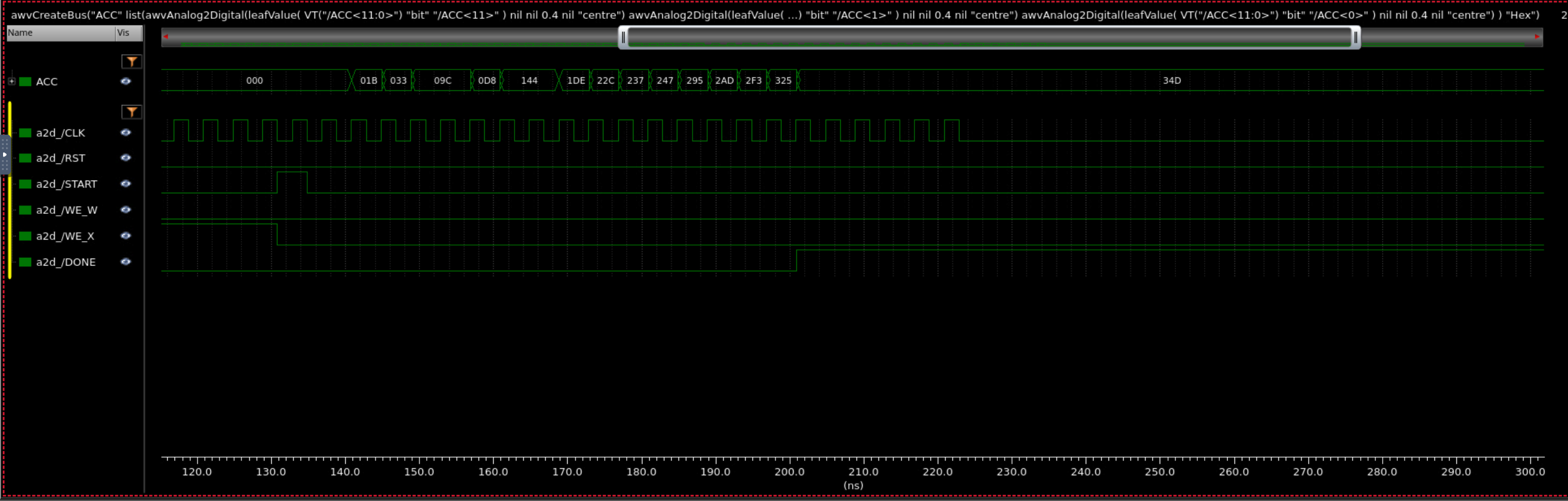
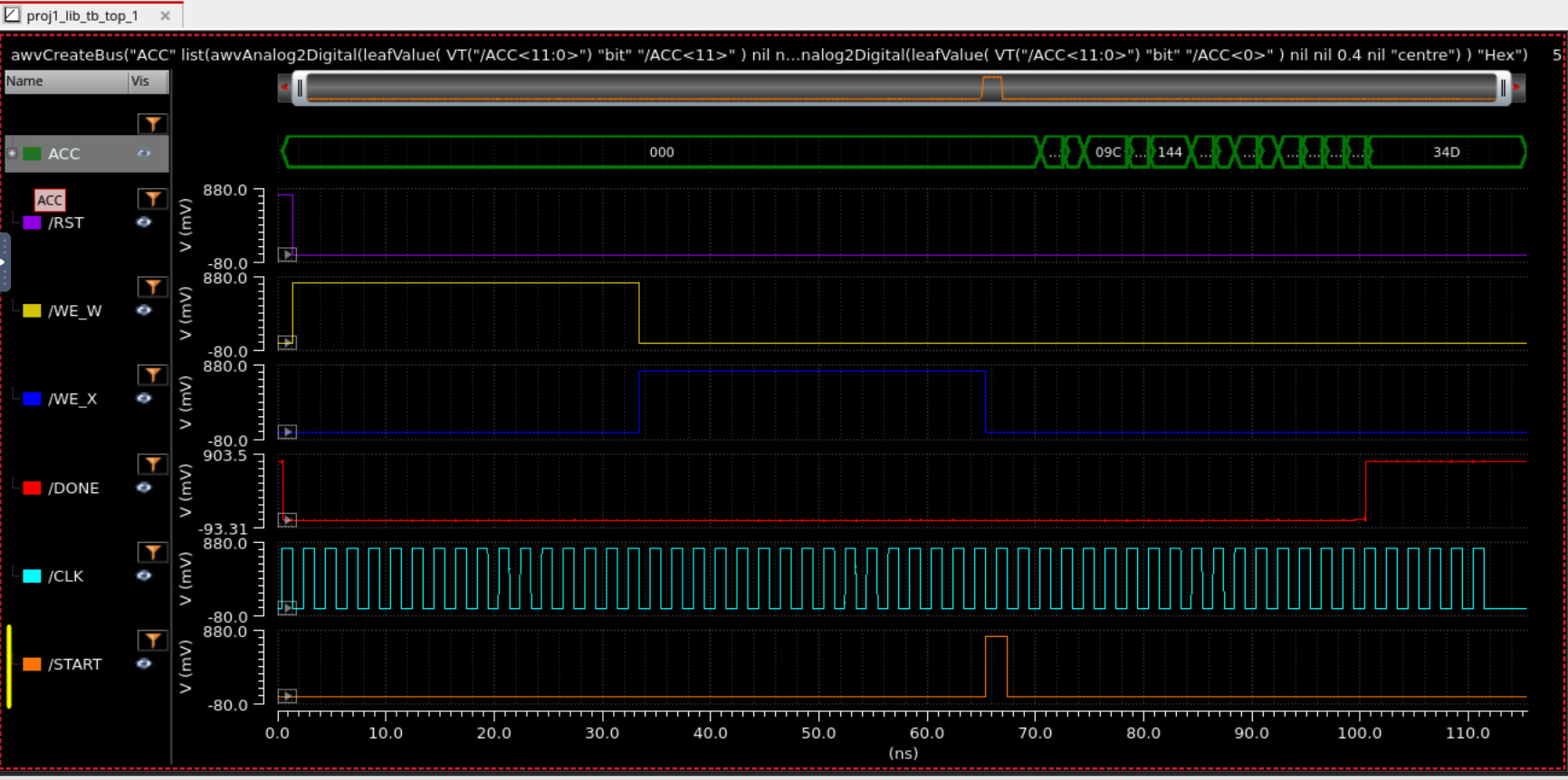
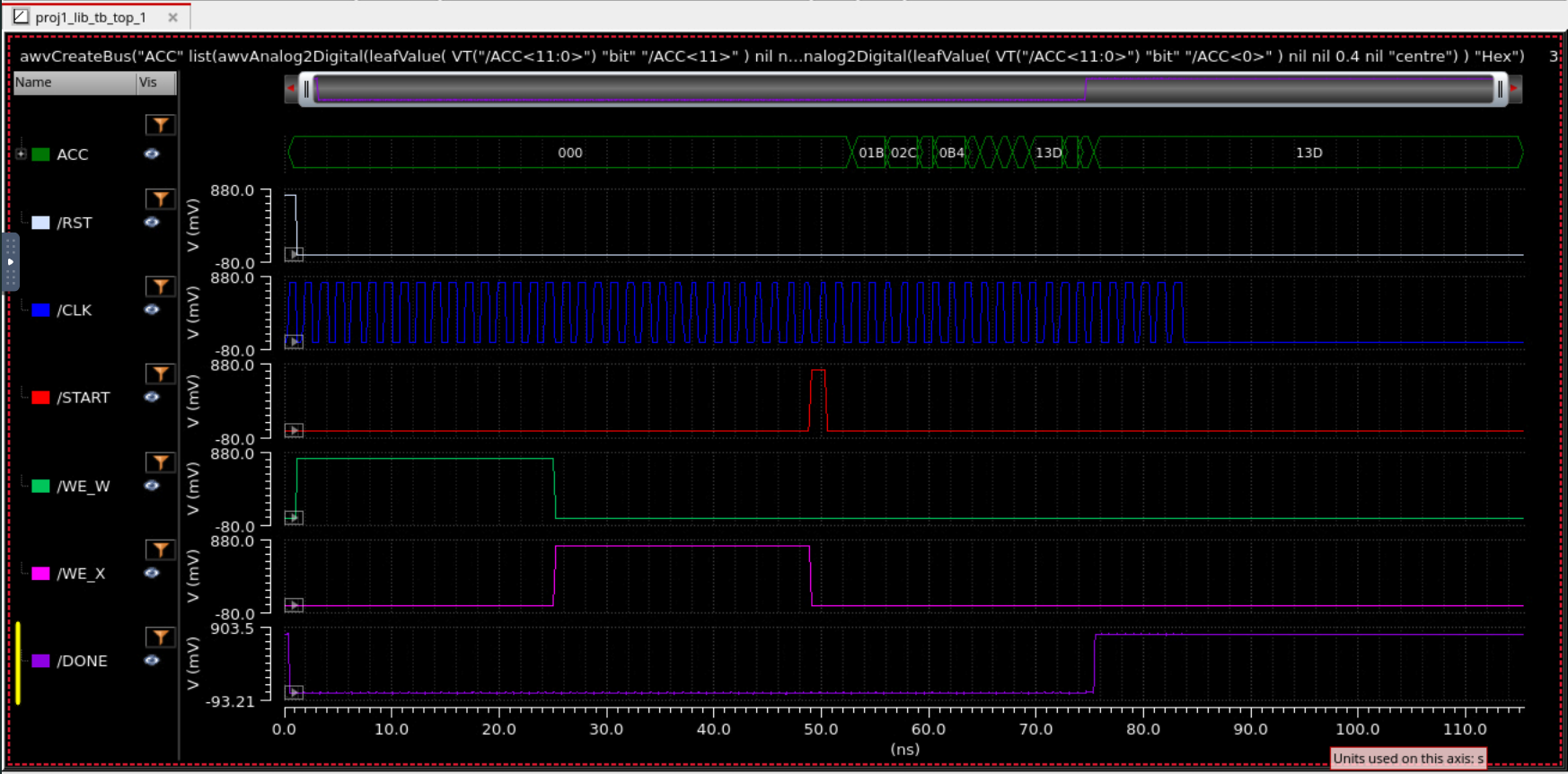
The first tb_top runs finished DONE with ACC = 0: RD_EN was a ~150 ps pulse that closed before RD crossed mid-rail. RD_EN is now CLKBUF · not WE_L (level-sensitive on clock-high). Tests A–C after the fix are the check.
9.5. Energy and FOM
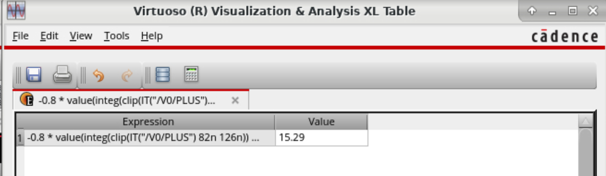
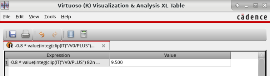
Single VDD pin on tb_top. Window 82–126 ns (44 ns clip; latency is 42.5 ns).
| Test | ACC | \(E_{dot}\) (meas.) | \(E_{\mathrm{MAC}}=E_{dot}/16\) |
|---|---|---|---|
A |
0x34D |
8.870 pJ |
0.5544 pJ/MAC |
B |
0xE10 |
15.29 pJ |
0.9556 pJ/MAC |
C |
0x320 |
9.500 pJ |
0.5938 pJ/MAC |
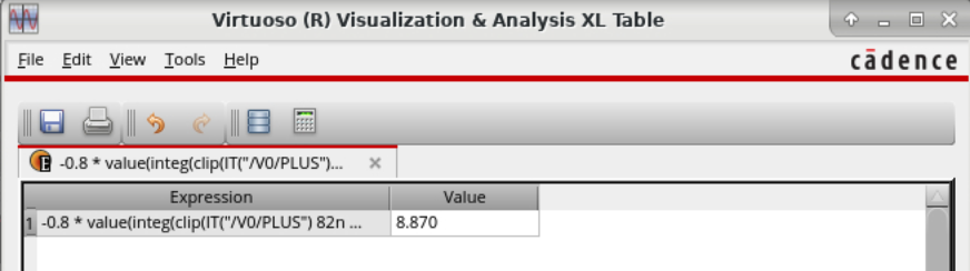
Memory vs logic is not a second Spectre split (one VDD). From Part 2: \(E_{\mathrm{macro/cyc}}\approx86.7\) fJ at 2.5 ns → \(E_{\mathrm{mem}}\approx2.77\) pJ (est.) for two macros × 16 addresses. Test A logic ≈ 6.10 pJ (0.38 pJ/MAC without memory, est.). Bitline restore is only 0.29 pJ of that 2.77 pJ; the clocked Part 2 controller dominates.
reported as \(1.1\times10^{5}\) µm²·pJ·ns.
9.6. What limited the design
The period is set by the multiply-accumulate path (~1.2 ns multiplier, then 12-bit ripple and \(t_{su}=40\) ps), not the 488 ps SRAM read. Ripple arithmetic was kept for one verified full adder. A chip-select on the macros would cut the clocked memory energy; a pipeline register after the multiplier would split SRAM and arithmetic at a second extra cycle (18).
10. Verification
Part 1 numbers that come from Quantus are extracted. Part 2 (sram_macro) and Part 3 (top) in this report are schematic-level Spectre benches: no DRC, LVS, or PEX on the macro or the MAC. Area outside the tiled cell uses \(D=28\) from Part 1.
10.1. Signoff that actually ran
| Part | Layout / extraction | Simulation |
|---|---|---|
1 bitcell |
DRC 0, LVS clean, Quantus C+CC |
Extracted hold / read SNM, write margin, cell current, supply sweep |
2 SRAM macro |
none (tiled-cell area only) |
|
3 MAC |
none |
|
10.2. Benches that exist
-
Part 1: butterfly (hold and read), write-margin sweep, cell current, 0.8 / 0.7 / 0.5 V supply table, functional write/read with 15-load bitlines (Cell schematic and dimensions, Read-SNM experiment and evidence, Layout, extraction and post-layout results).
-
Part 2: write driver nfin sweep, decoder address-to-WL,
tb_sram_macrocheckerboard / complement / worst-row, period sweep to 0.69 ns, power including standby (SRAM macro (Part 2)). -
Part 3 register:
tb_dffclock-to-Q, setup, hold, \(C_{CLK}\), idle/toggle energy. -
Part 3 datapath:
tb_multiplier4b256/256 products; 12-bit adder as twelve copies of the same full adder. -
Part 3 sequencer:
tb_controller_mac60/60,tb_counter4b38/38. -
Part 3 integration:
tb_topTests A (0x34D), B (0xE10), C (0x320) at 10 / 4.0 / 2.5 / 2.0 / 1.75 / 1.5 ns; VDD-pin energy at 2.5 ns (MAC unit (Part 3)).
10.3. Correctness properties
| Property | Where it is checked |
|---|---|
DRC 0, LVS match |
Part 1 cell only ( |
Extracted SNMread > 0 at 0.8 V and 0.7 V |
Part 1 butterflies (140 mV / 110 mV) |
Write 0 then read 0; write 1 then read 1 |
Part 1 functional check; Part 2 err1 / err2 / err3 |
DOUT matches written word |
|
256/256 products |
|
COUNT 0–15, DONE 17 edges after START |
|
ACC = Σ W[i]·X[i] on A/B/C |
|
10.4. Re-running locally
-
Open
proj1_libin Virtuoso (flow checkout in Specification). -
Part 1: check-and-save the schematic; DRC, LVS, PEX; ADE states in Cell schematic and dimensions and Read-SNM experiment and evidence.
-
Recompute read SNM without Cadence:
python3 scripts/check_snm_sweep.py --all # per-beta: results/part1/read-snm/beta*/raw.csv -> q.csv, qb.csv, snm.json, butterfly.png/.svg -
Part 2 / 3: schematic-level ADE on
tb_sram_macro,tb_dff,tb_multiplier4b,tb_controller_mac,tb_top. Vector files live instimuli/timing/on the cluster.
Raw 4-col SNM exports live in results/part1/read-snm/beta*/raw.csv. Part 2 notes: results/sram_macro_unit_test.md, results/sram_macro_area_fom.md. Part 3 figures: report/part3/img/.
11. Captured benches
Chapters above keep one or two figures per idea. This page is the rest of the captures worth keeping: FO4, decoder delay, err1/err2, DFF energy, Test B/C energy, leaf cells. Debug dumps (_unreadable, _overzoomed, _prefix) stay out. Full sets are in the Part 1, Part 2 and Part 3 PDFs.
On a phone the grid is one column; tap a capture for the full-size file.
11.1. Macro captures
inv_u, 53 ps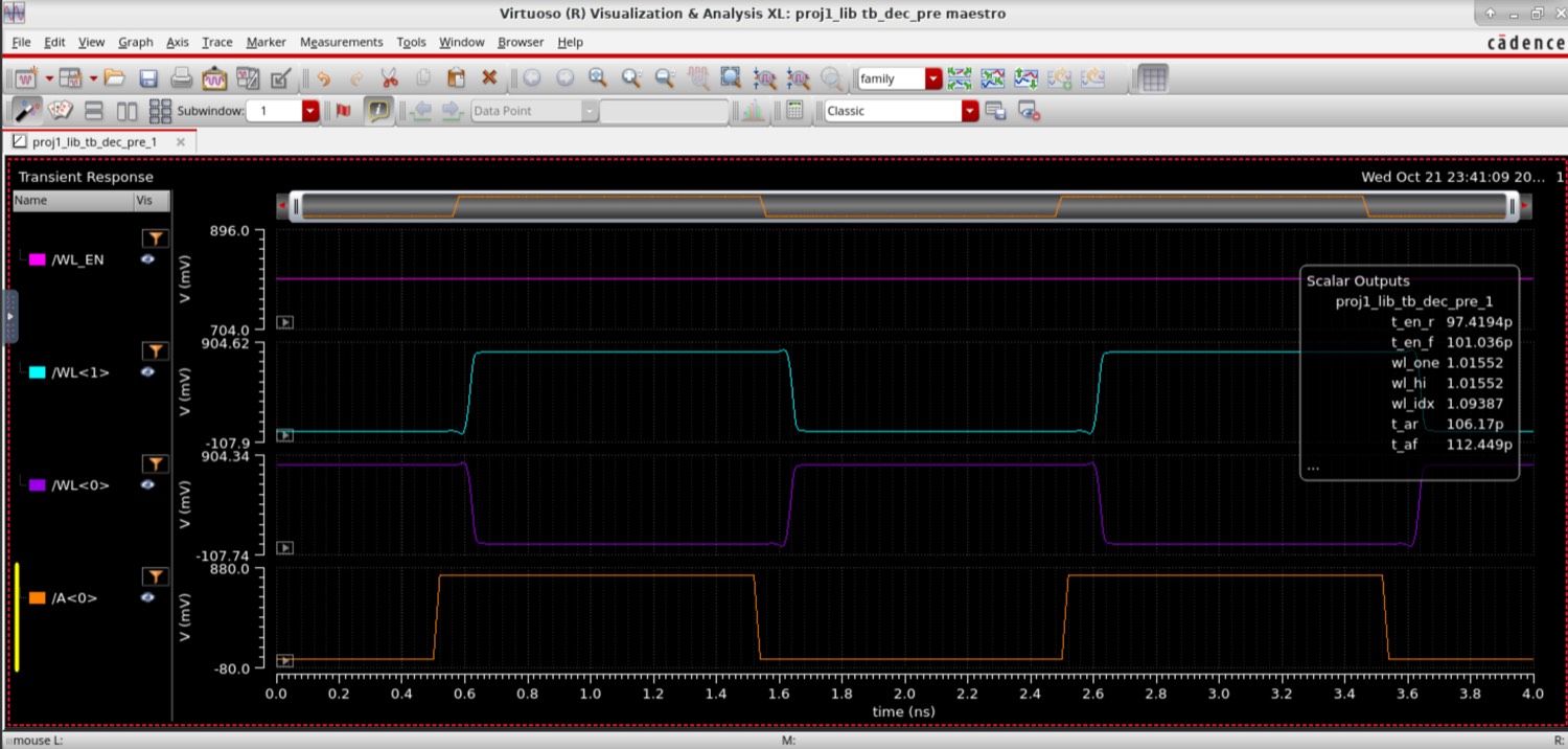
tb_sram_macro err1 / err2 pass11.2. MAC captures
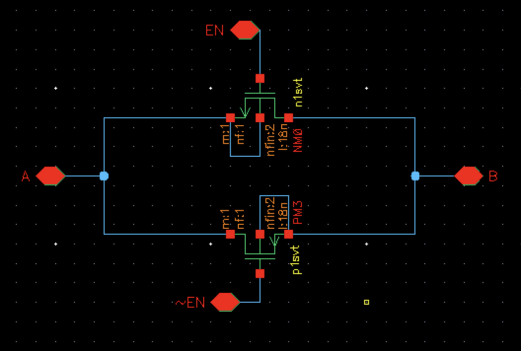
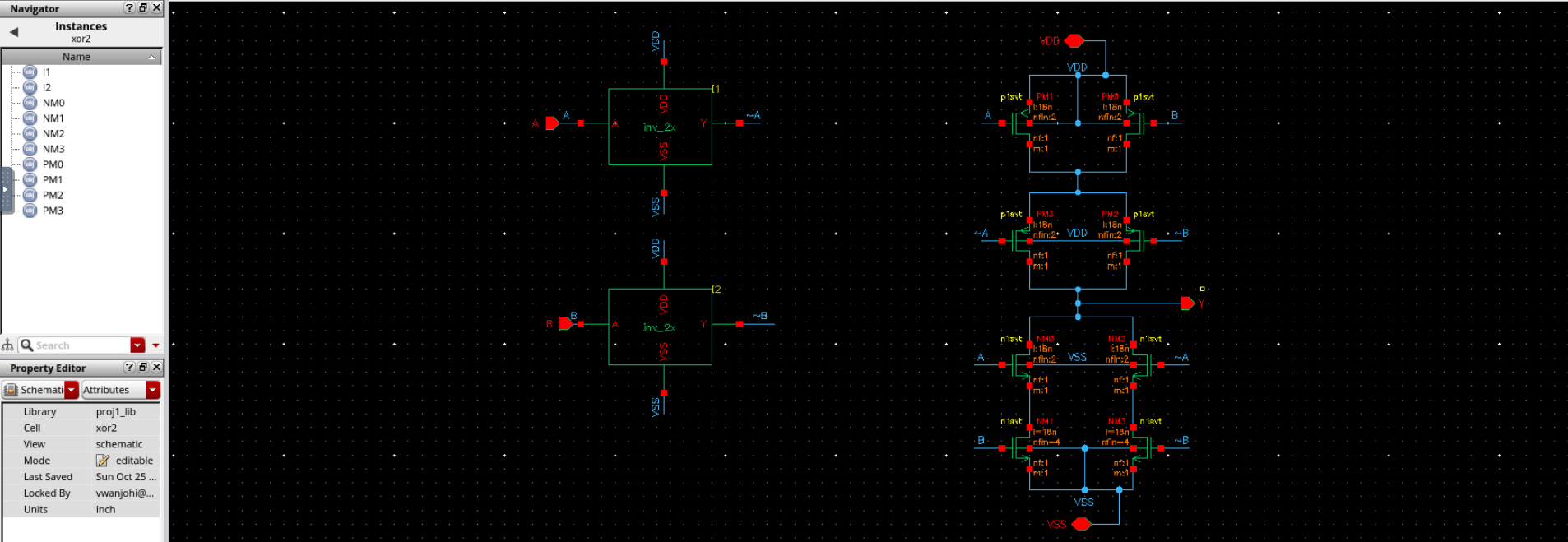
12. Sources, reproducibility and authors
This site is the HTML companion to the three Gradescope PDFs:
The assignment source is the nine-page handout. Part 1 due 10/13/2026, Part 2 10/20/2026, Part 3 10/27/2026. Cadence libraries stay on the cluster (proj1_lib); this repository keeps reports, figures, and scripts.
Part 1 SNM CSVs are under results/part1/read-snm/beta1/, beta1p5/ and beta2/ (raw.csv, transfer curves, snm.json). Cyan overlay coordinates come from the two lobes entries in each snm.json; the fitted margin is the smaller side. The script uses 16,001 voltage samples and checks against 4,001 samples. Images in media/part1/ retain the handwritten work and original ViVA views.
Part 2 cropped captures: report/part2/img/small/. Part 3 ViVA captures: report/part3/img/. This site stages a curated subset, not every dump.
Tyrone Marhguy and Victor Wanjohi are the report authors. Both are responsible for the whole design and report. Task split is in team contributions.
13. Authors
The Part 1–3 reports and this site are produced by the two-person team behind the bitcell, SRAM macro, and MAC. Both members are responsible for understanding the full design and report for every part.
13.1. Victor Wanjohi
Class of 2028, Computer Engineering, University of Pennsylvania.